
Recessed channel with separated ONO memory device

a memory device and channel technology, applied in the field of memory devices, can solve the problems of reducing the density of data storage, reducing the speed and cost, affecting the performance of memory cells, and reducing the number of channels, so as to facilitate multi-bit operation, reduce the effect of short channel effects, and facilitate programming and erasure of memory cells

Active Publication Date: 2006-06-27
MONTEREY RES LLC
View PDF8 Cites 33 Cited by
  • Summary
  • Abstract
  • Description
  • Claims
  • Application Information

AI Technical Summary

Benefits of technology

[0015]The present invention provides systems and methods of fabricating a U-shaped memory device with a recessed channel and a segmented / separated ONO layer. Multibit operation is facilitated by the separated ONO layer, which includes a charge trapping region on sidewalls of polysilicon gate structures adjacent to source / drain regions. Programming and erasing of the memory cells is facilitated by the relatively short distance between acting source regions and the charge trapping regions associated with gate. Furthermore, short channel effects are mitigated by a relatively long U-shaped channel region that travels around the recessed polysilicon gate thereby adding a depth dimension to the channel length. This feature advantageously reduces short channel effects without sacrificing memory cell packing density.
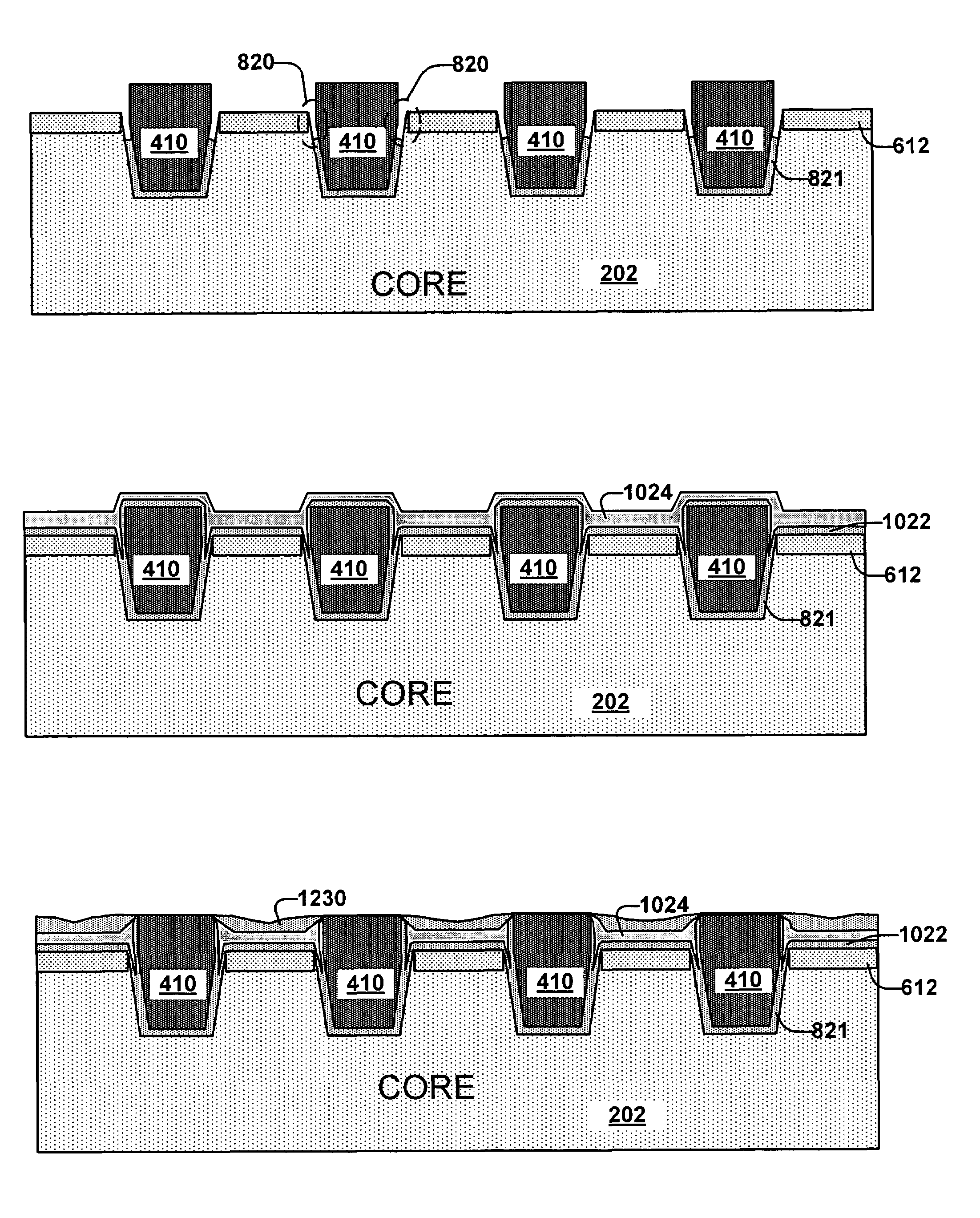
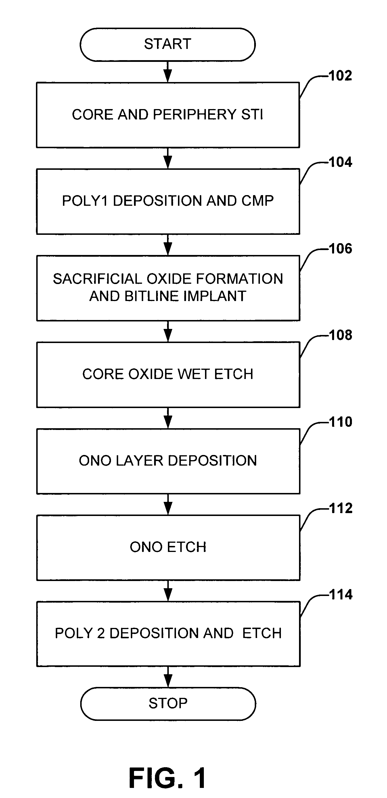
[0016]The U-shaped memory device of the present invention can be fabricated by forming recessed polysilicon gate structures. Gap regions are then created on sidewalls of the recessed polysilicon gate structure, wherein the gap regions are also adjacent to bitlines or source / drain regions. The gap regions are then filled with a charge trapping layer such as oxide-nitride-oxide (ONO). A second polysilicon layer can be selectively formed over the device to operate as wordlines and contacts can be formed to access the bit lines and thereby facilitate programming and reading the individual memory cells.

Problems solved by technology

For example, DRAM and SRAM allow individual bits of data to be erased one at a time, but such memory loses its data when power is removed.
EEPROM can alternatively be easily erased without extra exterior equipment, but has reduced data storage density, lower speed, and higher cost.
As device sizes and features are continually scaled down, however, leakage currents, cross talk and other issues can arise.
Shortening the channel in such a manner can, however, lead to short channel effects such as leakage currents as well as other undesirable performance issues.
For example, charge or bit isolation between the two bits stored in the charge trapping layer (e.g., nitride) becomes increasingly difficult as the channel length is decreased and the bits are brought closer together.

Method used


Image

  • Recessed channel with separated ONO memory device
  • Recessed channel with separated ONO memory device
  • Recessed channel with separated ONO memory device

Examples


Embodiment Construction

[0039]One or more aspects of the present invention are described with reference to the drawings, wherein like reference numerals are generally utilized to refer to like elements throughout, and wherein the various structures are not necessarily drawn to scale. In the following description, for purposes of explanation, numerous specific details are set forth in order to provide a thorough understanding of one or more aspects of the present invention. It may be evident, however, to one skilled in the art that one or more aspects of the present invention may be practiced with a lesser degree of these specific details. In other instances, well-known structures and devices are shown in block diagram form in order to facilitate describing one or more aspects of the present invention.

[0040]The present invention provides systems and methods of fabricating a U-shaped memory device with a recessed channel and a segmented / separated ONO layer. The memory device mitigates short channel effects, ...


PUM


Abstract

Systems and methods of fabricating a U-shaped memory device with a recessed channel and a segmented / separated ONO layer are provided. Multibit operation is facilitated by a separated ONO layer, which includes a charge trapping region on sidewalls of polysilicon gate structures adjacent to source / drain regions. Programming and erasing of the memory cells is facilitated by the relatively short distance between acting source regions and the gate. Additionally, short channel effects are mitigated by a relatively long U-shaped channel region that travels around the recessed polysilicon gate thereby adding a depth dimension to the channel length.

Description

FIELD OF INVENTION[0001]The present invention relates generally to memory devices and the like, and in particular fabricating a U-shaped memory device that has a recessed channel with a separated ONO layer thereby facilitating scaling and increased packing density.BACKGROUND OF THE INVENTION[0002]Many different types and styles of memory exist to store data for computers and similar type systems. For example, random access memory (RAM), dynamic random access memory (DRAM), static random access memory (SRAM), read only memory (ROM), programmable read only memory (PROM), electrically programmable read only memory (EPROM), electrically erasable programmable read only memory (EEPROM) and flash memory are all presently available to accommodate data storage.[0003]Each type of memory has its own particular advantages and disadvantages. For example, DRAM and SRAM allow individual bits of data to be erased one at a time, but such memory loses its data when power is removed. EEPROM can altern...

Claims


Application Information

Patent Timeline
Patent Type & Authority Patents(United States)
IPC IPC(8): H01L21/336
CPCH01L27/105H01L27/11568H01L29/7923H01L29/66833H01L29/792H01L29/42352H10B43/30
Inventor PARK, JAEYONGSHIRAIWA, HIDEHIKOTORII, SATOSHIRAMSBEY, MARK T.
Owner MONTEREY RES LLC
Learn More