Semiconductor integrated circuit device and its manufacturing method

a technology of integrated circuit and semiconductor, which is applied in the direction of semiconductor devices, electrical equipment, transistors, etc., can solve the problems of deteriorating access speed, inability to design a large read current for each conventional cell, and several problems of foregoing memory cells, so as to improve the electrical reliability of a semiconductor integrated circuit, improve the read current, and reduce the cell area.

Inactive Publication Date: 2006-06-27
RENESAS ELECTRONICS CORP
View PDF16 Cites 22 Cited by
  • Summary
  • Abstract
  • Description
  • Claims
  • Application Information

AI Technical Summary

Benefits of technology

[0015]It is therefore an object of the present invention to provide a semiconductor integrated circuit device which allows a significant increase in the read current for a nonvolatile memory using a nonconductive trap film as a charge accumulation region and allows the elimination of a read failure due to data inversion caused by a read disturb condition.
[0016]Another object of the present invention is to provide a device str

Problems solved by technology

However, the foregoing memory cells have several problems.
A first problem is that each of the conventional cells cannot be designed to allow a large read current.
This causes the problems of deterioration of the access speed and a lowering of the margin for misoperation of a se

Method used


Image

  • Semiconductor integrated circuit device and its manufacturing method
  • Semiconductor integrated circuit device and its manufacturing method
  • Semiconductor integrated circuit device and its manufacturing method

Examples


embodiment 1

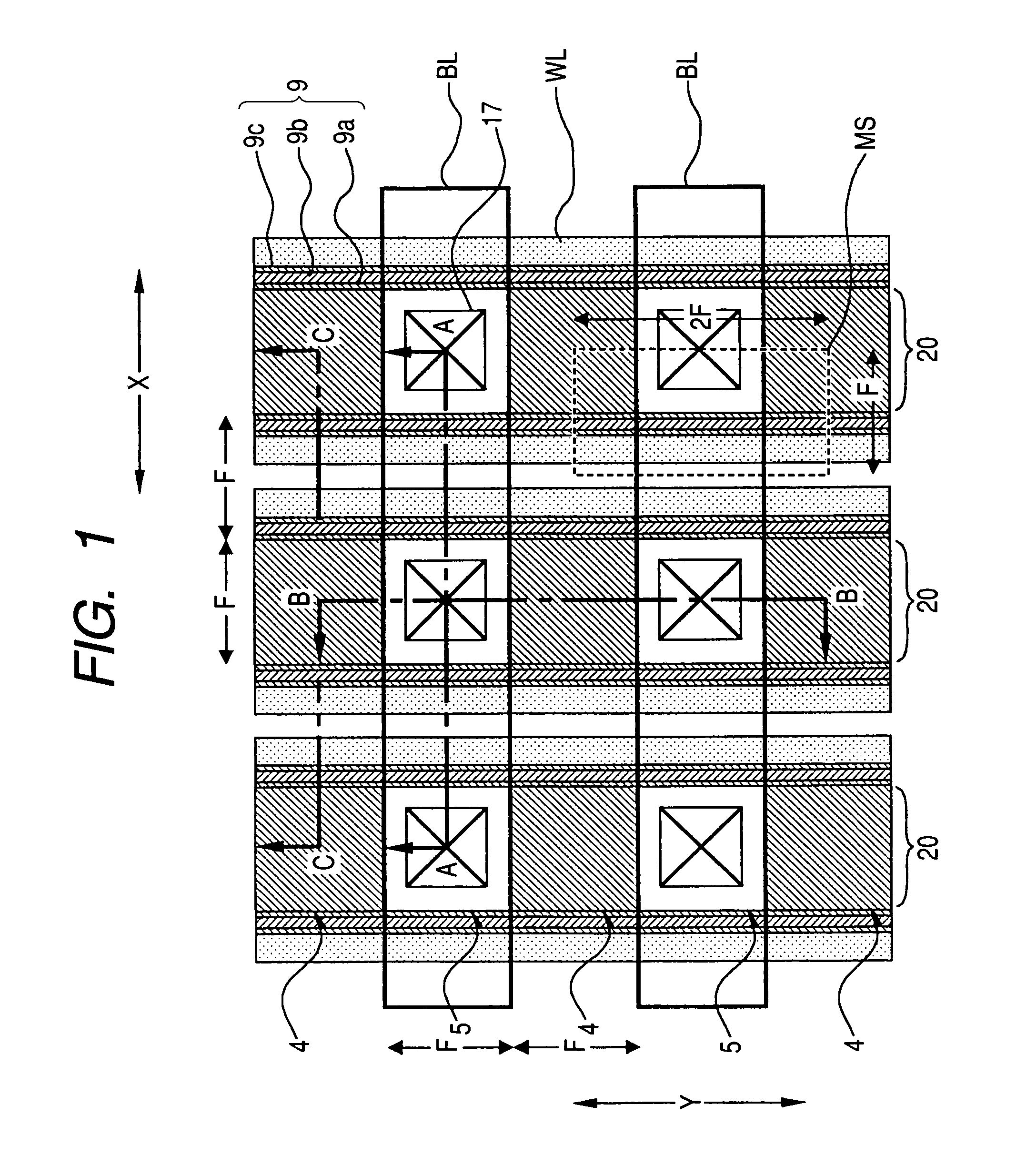
[0081]FIG. 1 is a diagrammatic plan view showing the structure of a memory cell array portion in a flash memory representing Embodiment 1 of the present invention.

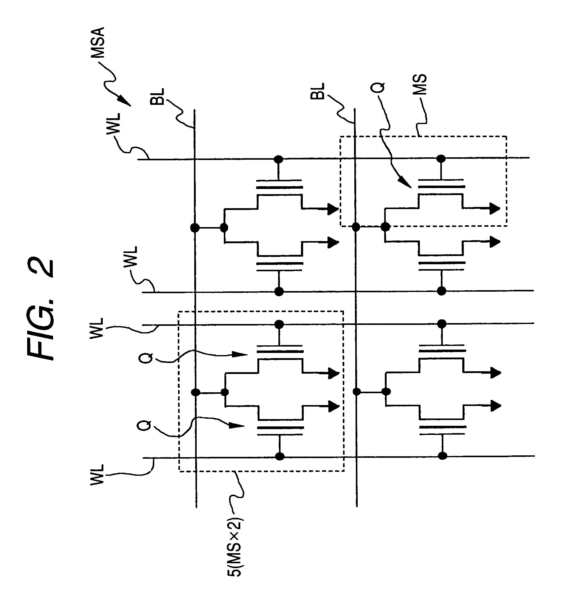
[0082]FIG. 2 is an equivalent circuit diagram of the memory cell array portion of FIG. 1.

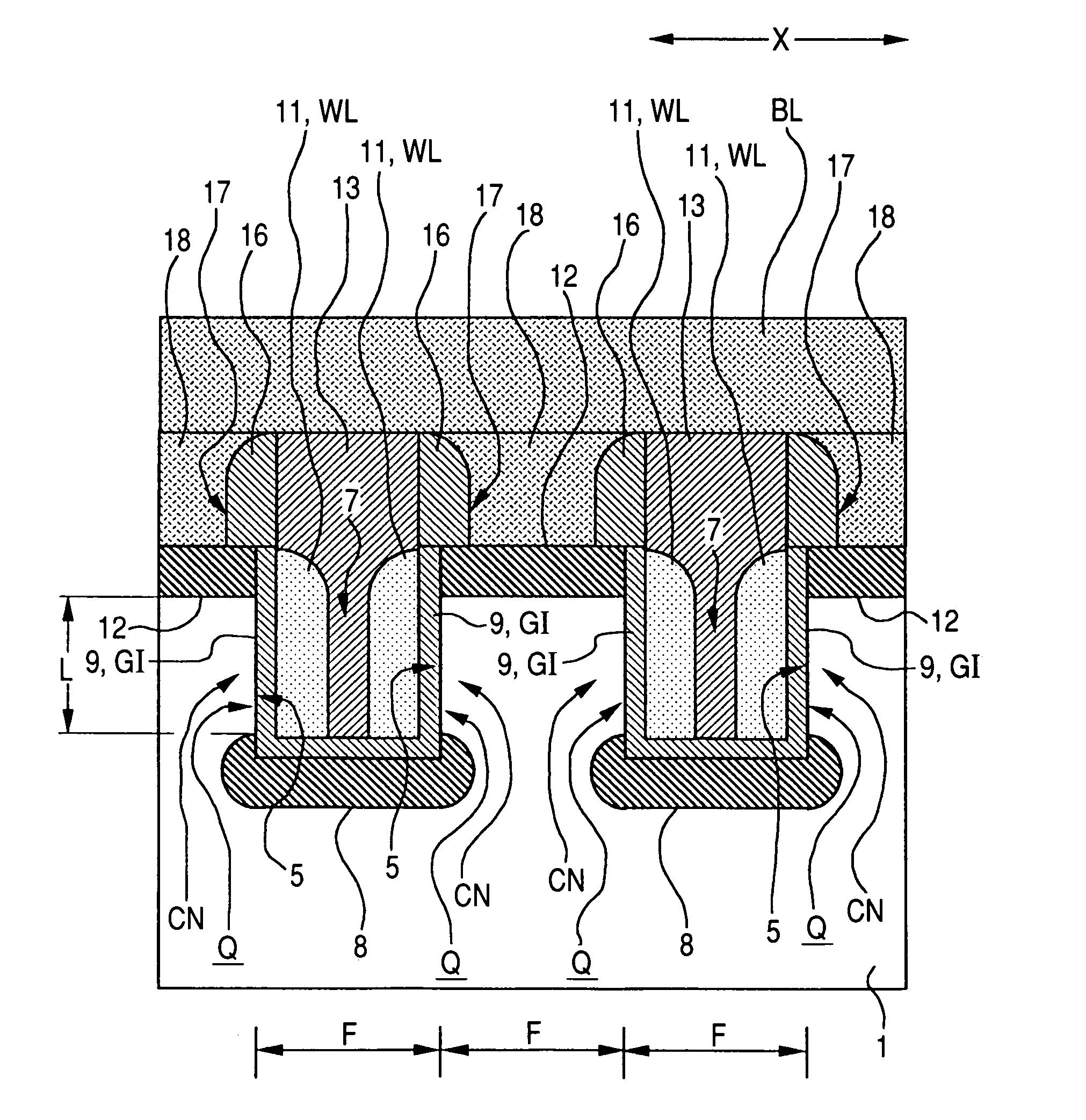
[0083]FIG. 3 is a diagrammatic cross-sectional view taken along the line A—A of FIG. 1.

[0084]FIG. 4 is a diagrammatic cross-sectional view obtained by enlarging a part of FIG. 1.

[0085]FIG. 5 is a diagrammatic cross-sectional view taken along the line B—B of FIG. 1.

[0086]FIG. 6 is a diagrammatic cross-sectional view taken along the line C—C of FIG. 1.

[0087]In the memory cell array portion MSA of the flash memory in the present embodiment, a plurality of word lines WL and a plurality of data lines BL extend, as shown in FIGS. 1 and 2. The plurality of word lines WL extend in the Y-direction and are arranged at a given spacing in the X-direction orthogonal to the Y-direction. The plurality of data lines BL extend in the X-direction and ar...

embodiment 2

[0111]The present embodiment pertains to the connection of electrodes to the control gate electrodes formed as side spacers in the memory cells according to the present application. In FIGS. 23 and 24, plan views of the nonvolatile memory cells according to the present invention are shown schematically. In the drawings, an electrode connecting structure to the control gate electrodes at the edge portions of a memory array is shown, in which rectangular-parallelepiped semiconductor pillars 41 are arranged and trenched isolation regions (insulator pillars) 42 are formed such that every second of them is different in length at the edge portions of the memory array. In the processing of control gate electrodes 45 into side spacers, regions from which the control gate electrodes 45 are extracted are formed by using mask patterns 44 defining the gate electrode of a peripheral circuit and connected to first metal lines 48 via contact holes 47. The placement pitch of the control gate electr...

embodiment 3

[0124]The present embodiment pertains to a method of manufacturing memory cells according to the present invention and the transistor for the peripheral circuit in the same manufacturing process steps, which will be described with reference to the cross-sectional views in the individual manufacturing process steps shown in FIGS. 25 to 33. Each of the cross-sectional views shows a cross section of a peripheral circuit portion and a memory cell portion.

[0125]First, FIG. 25 shows a state in which a trenched isolation region 52 is formed by filling an oxide film in a trench at a depth of 250 nm in a surface region of a p-type semiconductor silicon substrate (hereinafter simply referred to as a silicon substrate) 51 with a resistivity of 10 Ωcm and planarizing it by CMP (Chemical Mechanical Polishing), and, then, a surface oxide film 53 with a thickness of 10 nm is formed. Through the surface oxide film 53, an n-type well region has been formed by implanting phosphorus ions at an acceler...


PUM


Abstract

A semiconductor integrated circuit device has a plurality of rows of pillars, each row being composed of semiconductor pillars and insulator pillars alternately arranged in one direction with no gap therebetween, a plurality of nonvolatile memory elements provided individually in the plurality of semiconductor pillars, the plurality of nonvolatile memory elements having control gate electrodes provided over side surfaces of said semiconductor pillars along the one direction via gate insulating films, drain regions provided in upper surface portions of the semiconductor pillars, and source regions provided in bottom surface portions of the semiconductor pillars, and lines including the respective control gate electrodes of the plurality of nonvolatile memory elements and provided along the one direction over the side surfaces of the rows of pillars along the one direction.

Description

TECHNICAL FIELD[0001]The present invention relates to a semiconductor integrated circuit device and its manufacture; and, more particularly, the present invention relates to a technique which is effective when applied to a semiconductor integrated circuit device having a nonvolatile memory element to which electrical erasing and writing of data can be performed.BACKGROUND OF THE INVENTION[0002]In recent years, a nonvolatile memory device called a flash EEPROM (Electrically Erasable Programmable Read Only Memory), in which data stored therein can be erased electrically simultaneously in specified units and in which data can be written electrically, has drawn increased attention as a memory device for storing data and data for program composition. The flash EEPROM (hereinafter referred to as a flash memory) has a memory cell composed of an electrically erasable and writable nonvolatile memory element, so that it is possible to erase data or data for program composition once written in...

Claims


Application Information

Patent Timeline
IPC IPC(8): H01L29/76H01L21/336H01L21/8246H01L27/10H01L27/115H01L27/11531H01L27/11568H01L27/11573H01L27/11575H01L29/788H01L29/792
CPCH01L27/115H01L29/7926H01L29/792H01L27/11568H10B43/30H10B69/00
Inventor SHUKURI, SHOJI
Owner RENESAS ELECTRONICS CORP
Why Eureka
Try Eureka