

Semiconductor device and method of fabricating the same
- Summary
- Abstract
- Description
- Claims
- Application Information
AI Technical Summary
Benefits of technology
Problems solved by technology
Method used
Image

Examples
Embodiment Construction
[0069]Preferred embodiments in accordance with the present invention will be explained hereinbelow with reference to drawings.
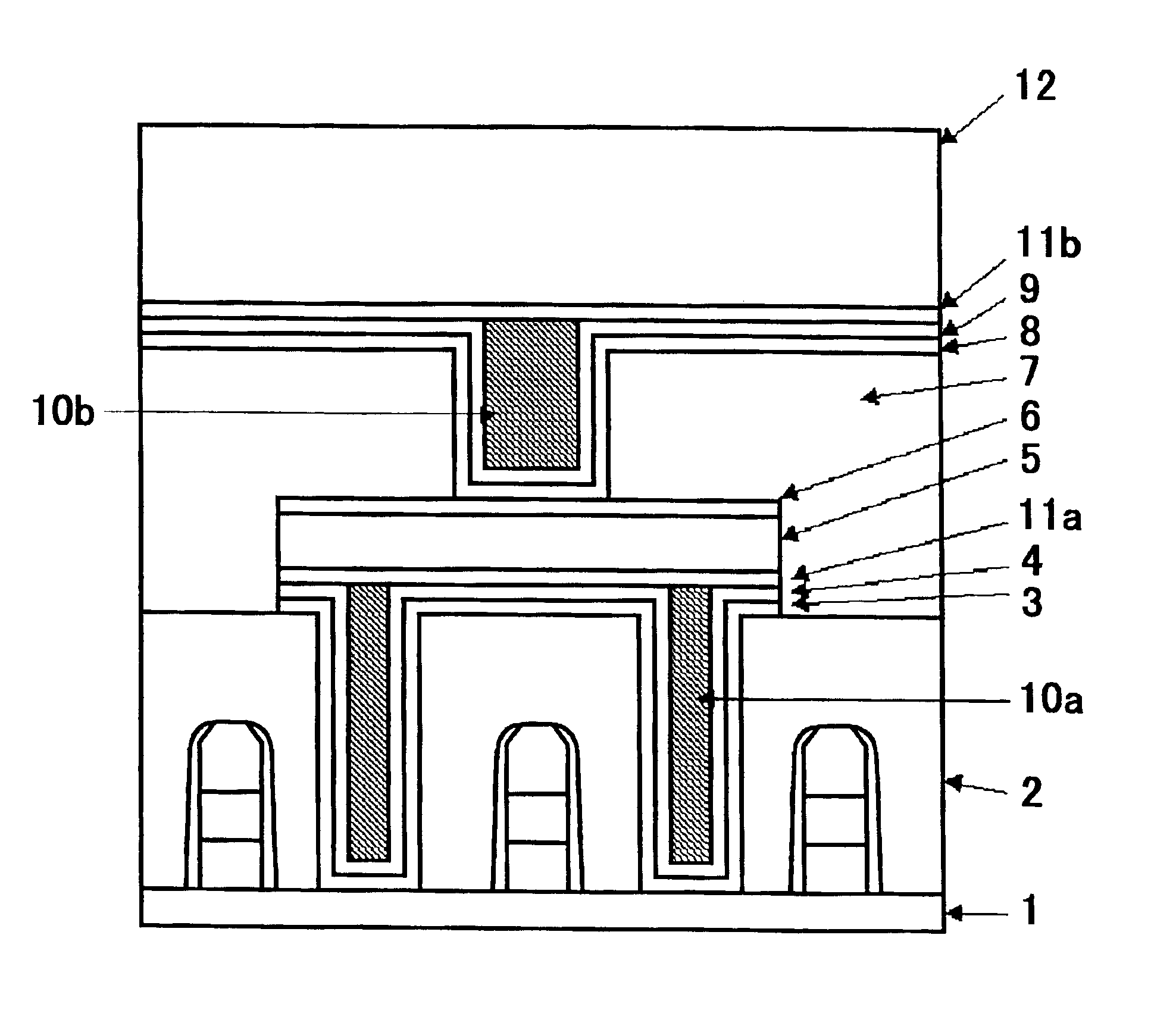
[0070]FIG. 4 is a cross-sectional view of a wiring structure in a semiconductor device in accordance with the first embodiment.
[0071]The semiconductor device is comprised of a silicon substrate 1, a first electrically insulating film 2 composed of silicon dioxide and formed on the silicon substrate 1, a first titanium film 3 formed on the first electrically insulating film 2, a first titanium nitride film 4 formed on the first titanium film 3, a first aluminum-copper alloy film 5 formed as a lower wiring layer on the first titanium nitride film 4, a second titanium nitride film 6 formed on the first aluminum-copper alloy film 5, a second electrically insulating film 7 composed of silicon dioxide and formed on the second titanium nitride film 6, a second titanium film 8 covering an inner surface of a through-hole 7a formed throughout the second electrically in...
PUM
 Abstract
Description
Claims
Application Information