Method of transporting and processing substrates in substrate processing apparatus

Active Publication Date: 2006-06-27
DAINIPPON SCREEN MTG CO LTD
View PDF3 Cites 25 Cited by
  • Summary
  • Abstract
  • Description
  • Claims
  • Application Information

AI Technical Summary

Benefits of technology

[0028]In the twelfth and fourteenth aspects of the present invention, when the substrates belonging to a plurality of substrate units different in transport setting are received into each cell by way of the common substrate inlet and are subjected to the intra-cell process in the common processing unit, a substrate made ready for outward transfer earlier is allowed to be transferred outwardly. This means that when the substrate transport path for each substrate unit is in a flow (branching flow) in the direction of branching into a plurality of transport paths, the substrate made ready for outward transfer earlier is allowed to be transferred outwardly if there is a processing unit the use of which is shared between the plurality of transport paths. In such a branching flow, the control of the substrate processing orders in the respective transport paths avoids the subsequent conflict between flows. Therefore, the throughput is improved without the occurrence of the conflict between the flows.
[0029]In the thirteenth and fifteenth aspects of the present invention, when the substrates belonging to a plurality of substrate units different in transport setting are received into each cell by way of

Problems solved by technology

The control algorithm in the method disclosed in Japanese Patent Application Laid-Open No. 7-283094 (1995) increases in complexity as the substrate processing apparatus increases in size.
It is therefore difficult to achieve high efficiency while maintaining the relia

Method used


Image

  • Method of transporting and processing substrates in substrate processing apparatus
  • Method of transporting and processing substrates in substrate processing apparatus
  • Method of transporting and processing substrates in substrate processing apparatus

Examples


Embodiment Construction

[0045]

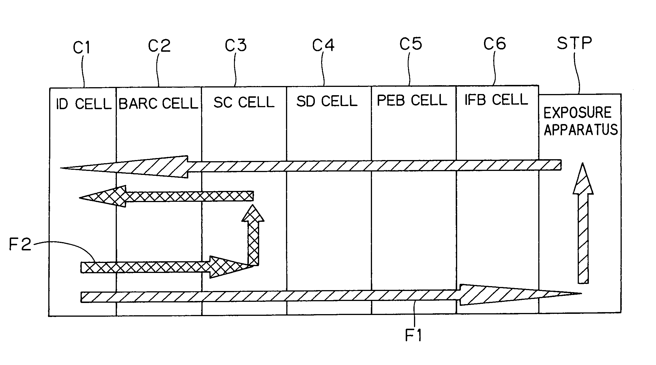
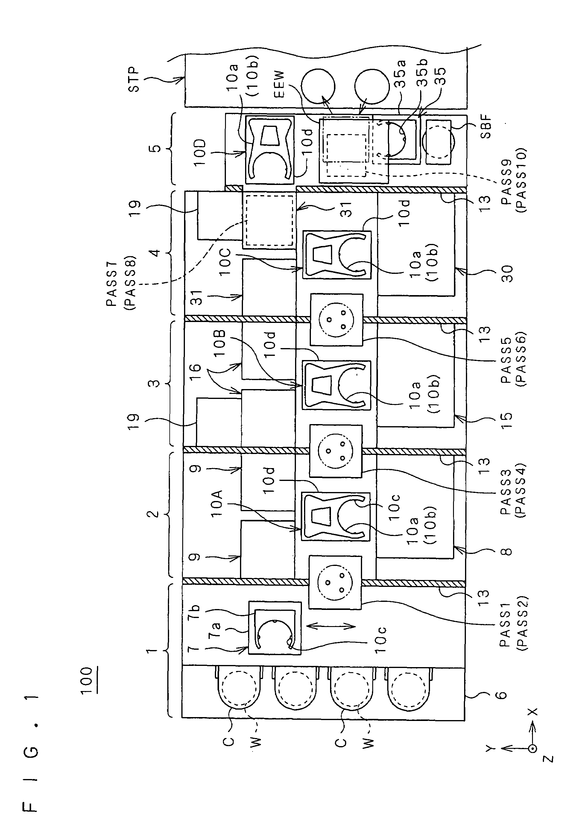
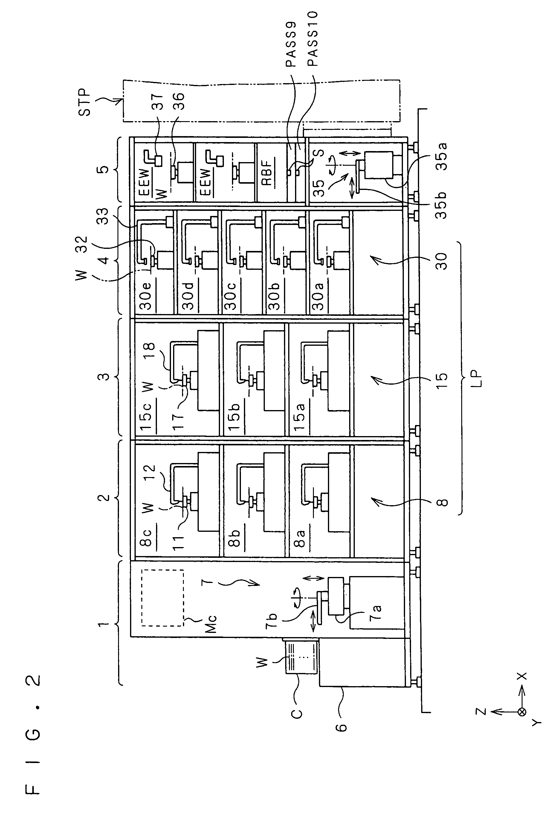
[0046]FIG. 1 is a plan view of a substrate processing apparatus 100 according to a preferred embodiment of the present invention. The substrate processing apparatus 100 is responsible for a resist coating process, a development process, their associated predetermined thermal and chemical processes, and the like for a photolithography process step for forming a predetermined circuit pattern on a semiconductor substrate (referred to simply as a “substrate”). A three-dimensional coordinate system is additionally shown in FIG. 1 in which a horizontal plane including an X axis defined to extend in the longitudinal direction of the substrate processing apparatus 100 is defined as an XY plane and a Z axis is defined to extend in a vertically upward direction.

[0047]As shown in FIG. 1, the substrate processing apparatus 100 according to the preferred embodiment principally comprises: an indexer block (ID block) 1; an anti-reflection film processing block (BARC block) 2; a resist film p...


PUM


Abstract

A substrate processing apparatus includes a plurality of cells each including a predetermined processing unit, a transport mechanism, and a cell controller. The cell controller independently controls operations in each cell in accordance with transport setting and processing condition setting for each cell described in recipe data determined for each substrate unit to be processed. Because the processing and transport are performed independently of the operations of adjacent cells, substrates belonging to different substrate units are received through a feed inlet or the same substrate inlet, are processed while being present in the same cell, and are transported to a feed outlet and a return outlet which are different substrate outlets. This allows the presence of different process flows in parallel.

Description

BACKGROUND OF THE INVENTION[0001]1. Field of the Invention[0002]The present invention relates to a method of transporting substrates including a semiconductor substrate, a glass substrate for a liquid crystal device and the like in a substrate processing apparatus including a plurality of processing units each for performing a predetermined process on these substrates.[0003]2. Description of the Background Art[0004]In a substrate processing apparatus which performs various processes on semiconductor substrates (or wafers), glass substrates and the like in the process steps of manufacturing semiconductor devices, liquid crystal devices and the like, attempts have been made at a multi-unit structure in which there are provided a plurality of processing units all responsible for a single process step and at a hybrid structure in which there are provided different types of processing units for performing a succession of different process steps in a single apparatus, thereby to respond t...

Claims


Application Information

Patent Timeline
IPC IPC(8): G06F19/00H01L21/677H01L21/00H01L21/027H01L21/67
CPCH01L21/67276
Inventor HASHINOKI, KENJIKOYAMA, YASUFUMIYAMADA, TAKAHARU
Owner DAINIPPON SCREEN MTG CO LTD
Why Eureka
Try Eureka