

Display panel drive circuit and display panel
- Summary
- Abstract
- Description
- Claims
- Application Information
AI Technical Summary
Benefits of technology
Problems solved by technology
Method used
Image

Examples
Embodiment Construction
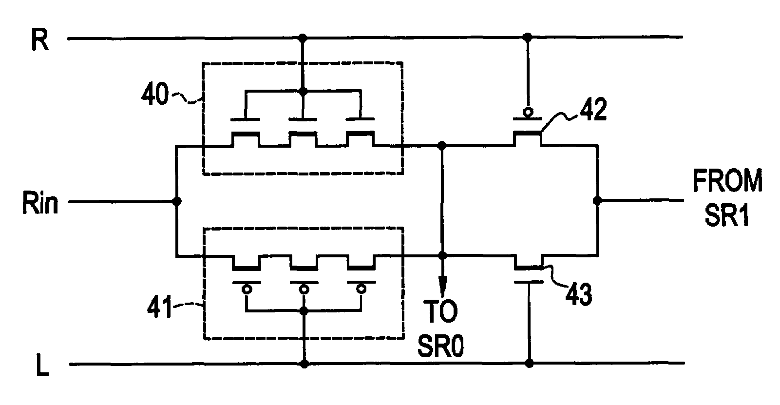
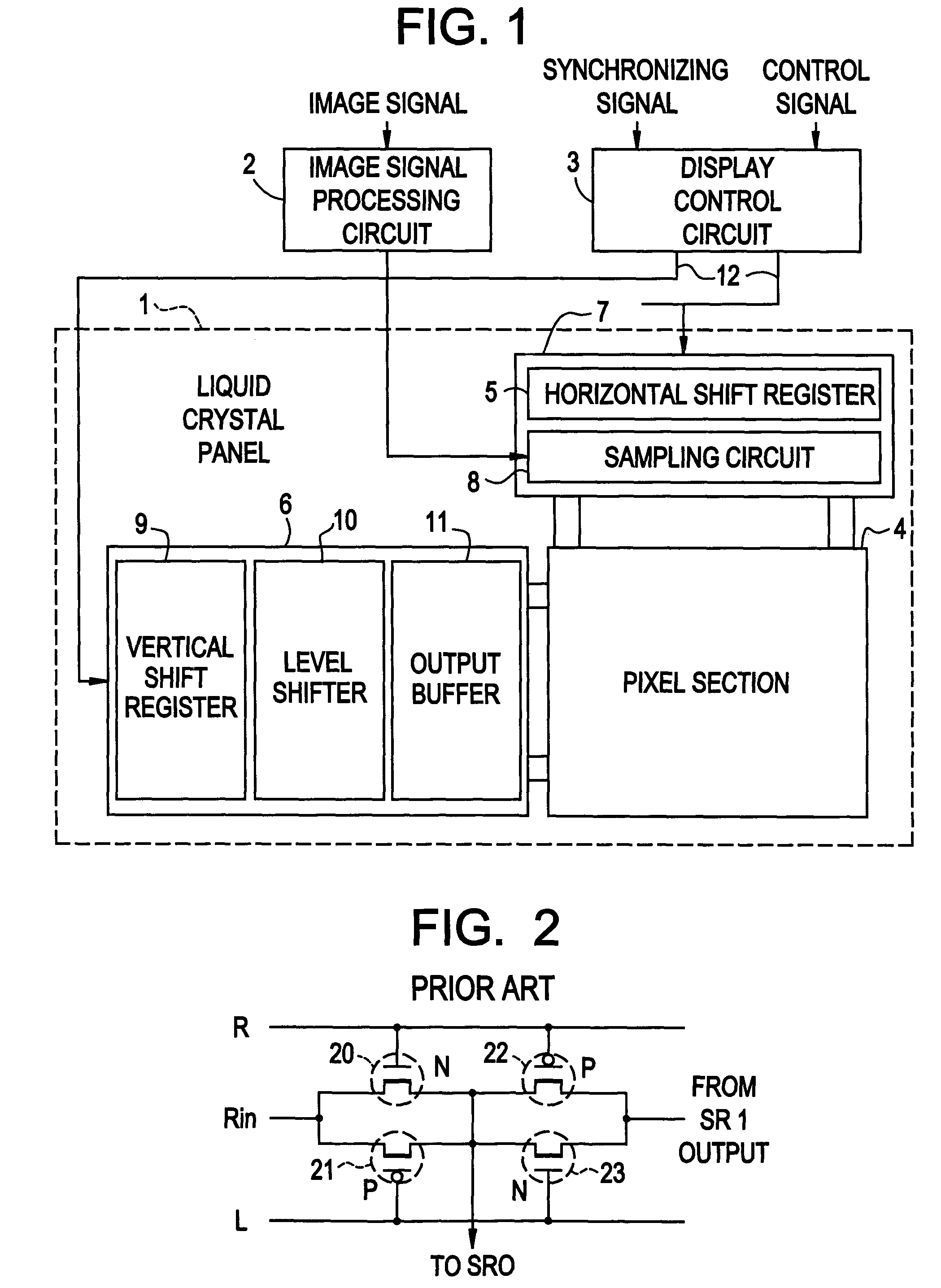
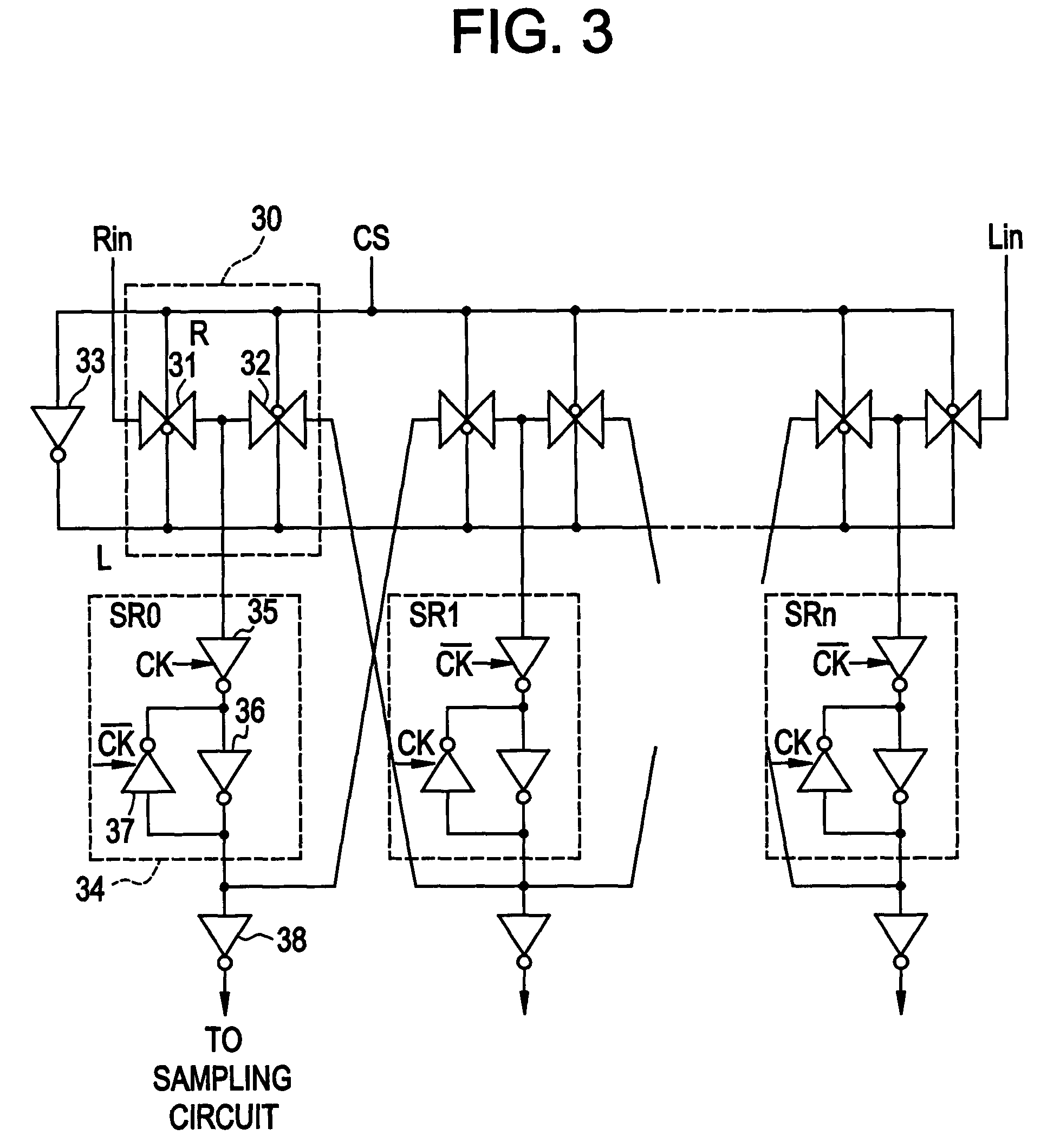
[0020]Now preferred embodiments according to the present invention will be described with reference to the drawings. FIG. 1 is a block diagram of a liquid crystal panel utilizing low-temperature polysilicon TFTs to which the present invention is applied. A liquid crystal panel 1 is integrally formed with a pixel section 4 formed by pixel TFTs arranged in a matrix form, and a horizontal scan circuit 5 and vertical scan circuit 6 both formed also by TFTs.
[0021]An image signal processing circuit 2 is inputted, for example, with a digital RGB signal to output an analog RGB signal required to drive the pixel section 4. A display control circuit 3 is inputted with an image synchronizing signal and a scan-direction control signal, and controls the horizontal scan circuit 5 and the vertical scan circuit 6. It is noted that the image signal control circuit 2, the display control circuit 3 and the like are mounted, for example, on a separate printed circuit board wherein the circuit board and...
PUM
 Abstract
Description
Claims
Application Information