Co-fired ceramic capacitor and method for forming ceramic capacitors for use in printed wiring boards

a ceramic capacitor and co-fired technology, applied in the manufacture of capacitors, fixed capacitor details, feed-through capacitors, etc., can solve the problems of low electrode stress, glass-ceramic does not re-soften and flow, and the surface of glass-ceramic is often difficult to adhere, so as to increase the capacitance density

Inactive Publication Date: 2006-07-04
CHEMTRON RES
View PDF25 Cites 33 Cited by
  • Summary
  • Abstract
  • Description
  • Claims
  • Application Information

AI Technical Summary

Benefits of technology

[0010]According to a first embodiment, a method for making a fired-on-foil ceramic capacitor structure comprises forming first dielectrics over a metallic foil, forming first electrodes over the first dielectrics, and co-firing the first dielectrics and the first electrodes. In the first embodiment, cracking and separation of the electrode from the dielectric caused by differences in thermal coefficient of expansion (TCE) between the electrodes and the dielectrics is avoided by co-firing the electrodes and the dielectrics. Alleviation of the TCE problem also allows the use of preferred materials, such as copper, to form the electrodes.
[0011]According to a second embodiment, a two-layer capacitor structure comprises a metallic foil, dielectrics disposed over the foil, first electrodes disposed over the first dielectrics, and second electrodes disposed over the dielectrics and over the first electrodes. In the second embodiment, the capacitance density of the capacitor structure is increased because of the additional dielectric / electrode layer. Additional layers may also be added, further increasing capacitance density. Also according to the second embodiment, the capacitor structure may comprise a copper foil and copper electrodes.

Problems solved by technology

The glass-ceramic, however, does not re-soften and flow on subsequent firings, and its surface is often difficult to adhere to.
Small TCE differences result in low stress in the electrode upon cooling from peak firing temperatures.
However, silver and silver-containing alloys may be undesirable in some applications because of the possibility of silver migration.
In addition, the relatively low melting points of silver and silver alloys preclude their use at higher firing temperatures.
Copper is a preferred material for forming electrodes, but the large TCE differences between copper and thick-film capacitor dielectrics lead to post-firing stresses in the electrodes.
The stresses result in electrode cracking.
In addition, because pre-fired glass ceramics do not re-soften and flow on subsequent firings, a copper electrode fired on a pre-fired glass-ceramic surface may not adhere well to the glass-ceramic.
Both cracking and separation result in high dissipation factors.

Method used


Image

  • Co-fired ceramic capacitor and method for forming ceramic capacitors for use in printed wiring boards
  • Co-fired ceramic capacitor and method for forming ceramic capacitors for use in printed wiring boards
  • Co-fired ceramic capacitor and method for forming ceramic capacitors for use in printed wiring boards

Examples


example 1

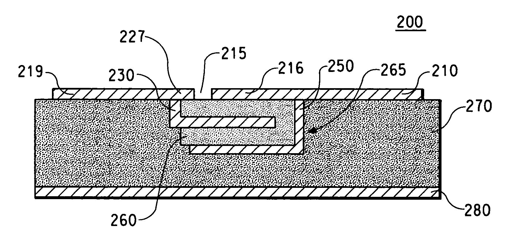
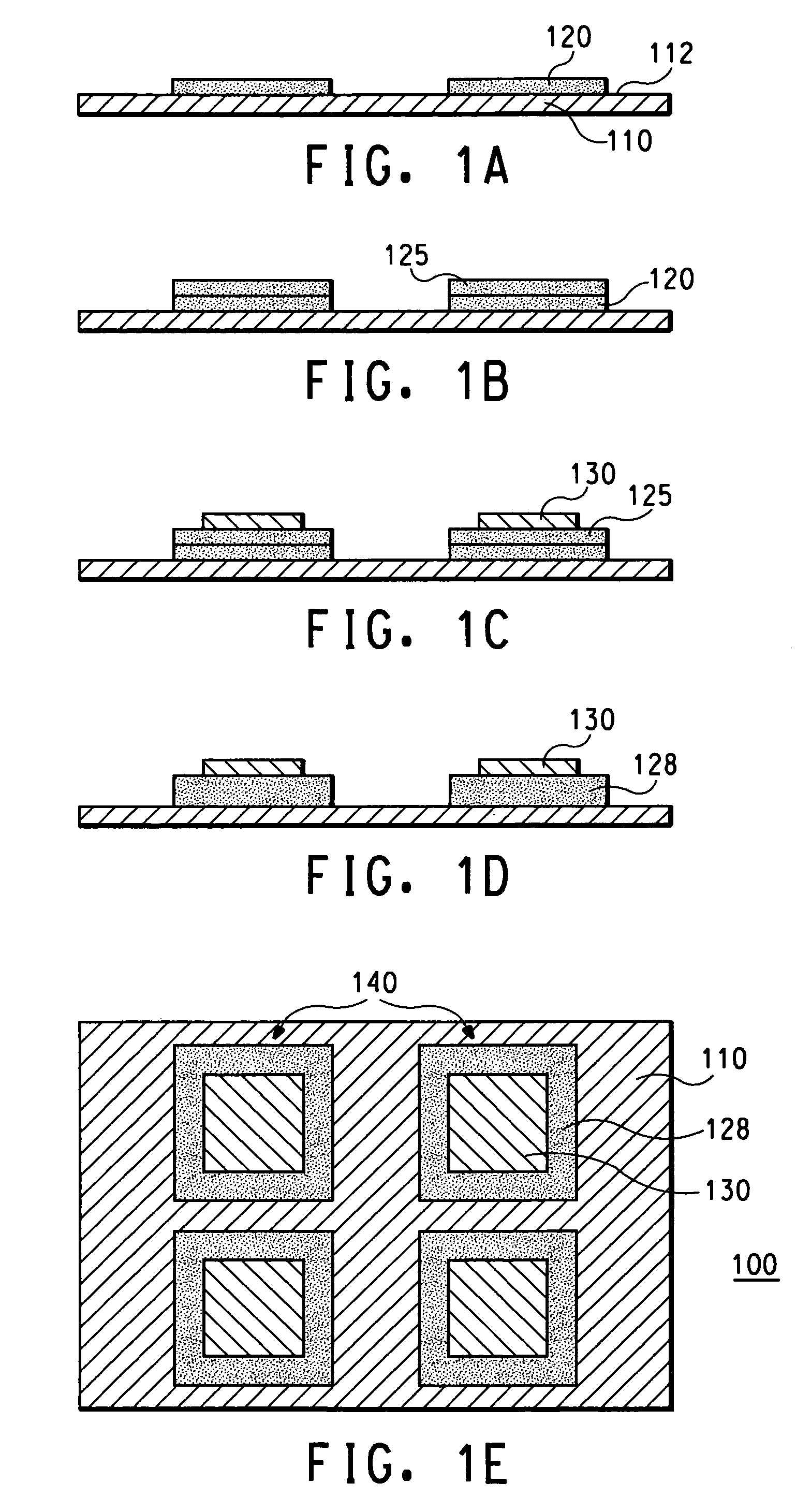
[0051]Referring to FIGS. 1A–1E, a specific embodiment of the capacitor structure 100 was described. In this embodiment, the foil 110 was a copper foil. The type of copper foil 110 can be any commercial grade of copper foil used in the printed wiring board industry, and may be in the range of ⅓ oz copper foil (approximately 12 microns thickness) to 1 oz copper foil (approximately 36 microns thickness). The copper foil 110 was pretreated by applying a copper underprint paste over selected areas of the foil 110. The resulting product was then fired in nitrogen at 900° C. for 10 minutes at peak temperature, with a total cycle time of approximately 1 hour, forming the underprint 112.

[0052]In FIG. 1B, a thick-film dielectric ink was screen-printed onto the pretreated copper foil 110 through 400 mesh screen to create a pattern of ½ inch by ½ inch first dielectric layers 120. The wet printed thickness of the first dielectric layers 120 is approximately 12–15 microns. The first dielectric la...

example 2

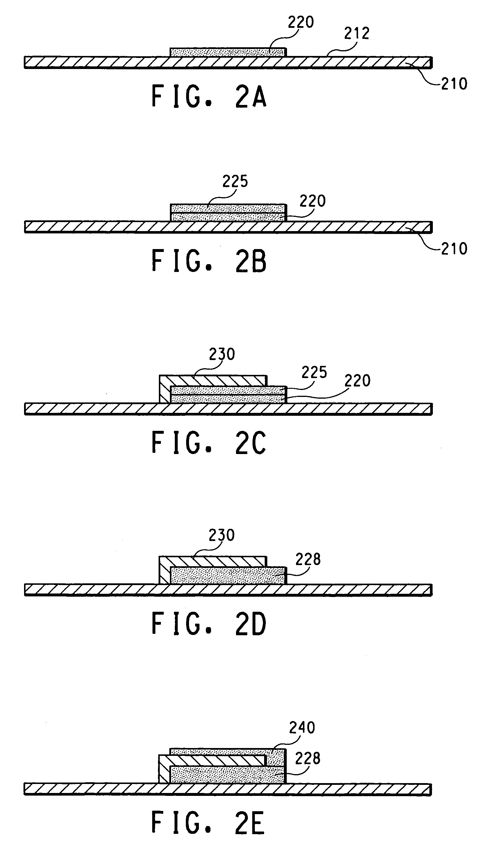
[0063]A process as described in Example 1 was repeated, except that the thick-film dielectric 128 was printed through 325 mesh screen, with a wet thickness of each of the two layers of approximately 15–20 microns. Results were similar to the embodiment of Example 1, except that the capacitance density was approximately 120 nF / inch2.

example 3

[0064]A process as described in Example 2 was repeated using a variety of dielectric and electrode dimensions shown in the table below:

[0065]

Dielectric Size milsElectrode Size mils250 × 250210 × 210 56 × 340 40 × 320176 × 340160 × 320 96 × 180 80 × 158 26 × 180 10 × 159176 × 180160 × 15836 × 9820 × 77 56 × 10040 × 78176 × 100160 × 78 36 × 5820 × 3796 × 6080 × 3836 × 3816 × 1726 × 3010 × 9  26 × 340 10 × 31890 × 9070 × 70330 × 330310 × 310119.5 × 119.5109.5 × 109.5 36 × 338 20 × 320 96 × 340 80 × 320 36 × 178 20 × 157336 × 180320 × 158 56 × 180 40 × 158 26 × 10010 × 74 56 × 10040 × 78 96 × 10080 × 7826 × 6010 × 3956 × 6040 × 3826 × 4010 × 1856 × 4040 × 1836 × 2820 × 7 336 × 340320 × 318170 × 170150 × 150240 × 240229.5 × 229.5

[0066]Capacitance in these embodiments was proportional to the area of the printed copper electrode, but the calculated capacitance densities were essentially identical to that of Example 1.


PUM

PropertyMeasurementUnit
thicknessaaaaaaaaaa
thicknessaaaaaaaaaa
thicknessaaaaaaaaaa

Abstract

A capacitor structure is fabricated by forming a pattern of first dielectrics over a foil, forming first electrodes over the first dielectrics, and co-firing the first dielectrics and the first electrodes. Co-firing of the dielectrics and the electrodes alleviates cracking caused by differences in thermal coefficient of expansion (TCE) between the electrodes and the dielectrics. Co-firing also ensures a strong bond between the dielectrics and the electrodes. In addition, co-firing allows multi-layer capacitor structures to be constructed, and allows the capacitor electrodes to be formed from copper.

Description

CROSS-REFERENCE TO RELATED DOCUMENT[0001]The present application is a division and claims the benefit of U.S. application Ser. No. 10 / 651,367, filed Aug. 29, 2003, which claims the benefit of Provisional Application 60 / 418,045, filed on Oct. 11, 2002.BACKGROUND[0002]1. Technical Field[0003]The technical field is ceramic capacitors. More particularly, the technical field includes co-fired ceramic capacitors that may be embedded in printed wiring boards.[0004]2. Background Art[0005]Passive circuit components embedded in printed wiring boards formed by fired-on-foil technology are known. Known components are separately fired-on-foil. “Separately fired-on-foil” capacitors are formed by depositing a thick-film dielectric material layer onto a metallic foil substrate and firing under thick-film firing conditions, and subsequently depositing a top electrode material over the thick-film dielectric material layer. U.S. Pat. No. 6,317,023 B1 to Felten discloses such a process.[0006]The thick-...

Claims


Application Information

Patent Timeline
Patent Type & Authority Patents(United States)
IPC IPC(8): H01G4/005H01G4/01H01G4/12H01G13/00H05K1/09H05K1/16H05K3/20H05K3/42H05K3/46
CPCH01G4/01H05K1/162H05K1/092H05K3/429H05K3/4611Y10T29/4913H05K2201/0355H05K2201/09509H05K2201/09718H05K2201/09763H05K3/4623H01G4/12
Inventor BORLAND, WILLIAM J.
Owner CHEMTRON RES
Why Eureka
Try Eureka