Doping of semiconductor fin devices

Active Publication Date: 2006-07-11
TAIWAN SEMICON MFG CO LTD
View PDF59 Cites 125 Cited by
  • Summary
  • Abstract
  • Description
  • Claims
  • Application Information

AI Technical Summary

Benefits of technology

[0006]The preferred embodiment of the present invention provides several methods for doping the semiconductor fin in a multiple-gate transistor to provide improve

Problems solved by technology

Consequently, a transistor with a short gate length suffers from problems related to the inability of the gate to substantially control the on and off states of the channel.
However, for device scaling well into the sub-50 nm regime,

Method used


Image

  • Doping of semiconductor fin devices
  • Doping of semiconductor fin devices
  • Doping of semiconductor fin devices

Examples


Example

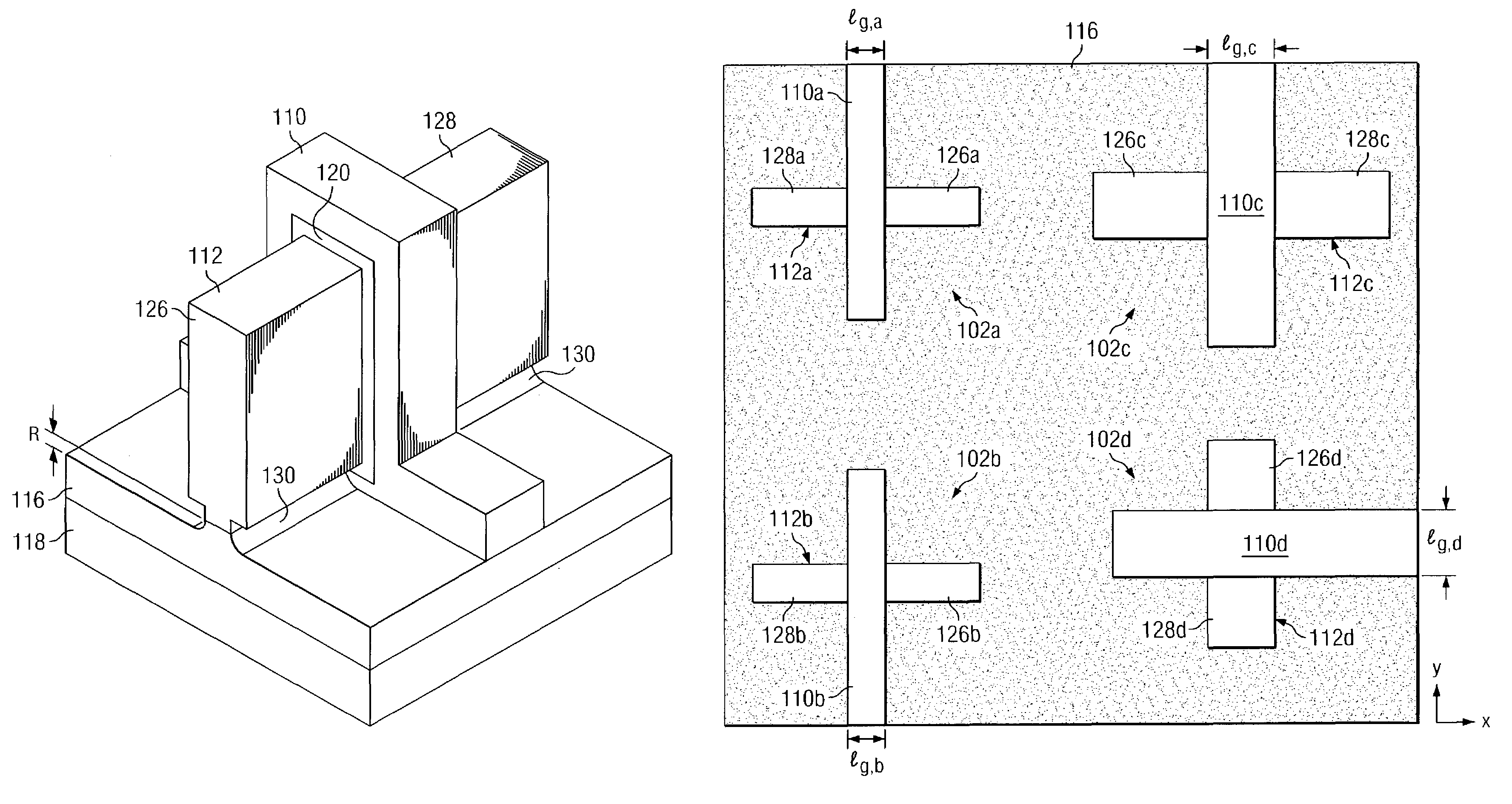
[0028]The preferred embodiment of the present invention relates to the field of semiconductor devices and more particularly to semiconductor devices with a fin structure. The present invention provides several methods for doping the semiconductor fin in a multiple-gate transistor.

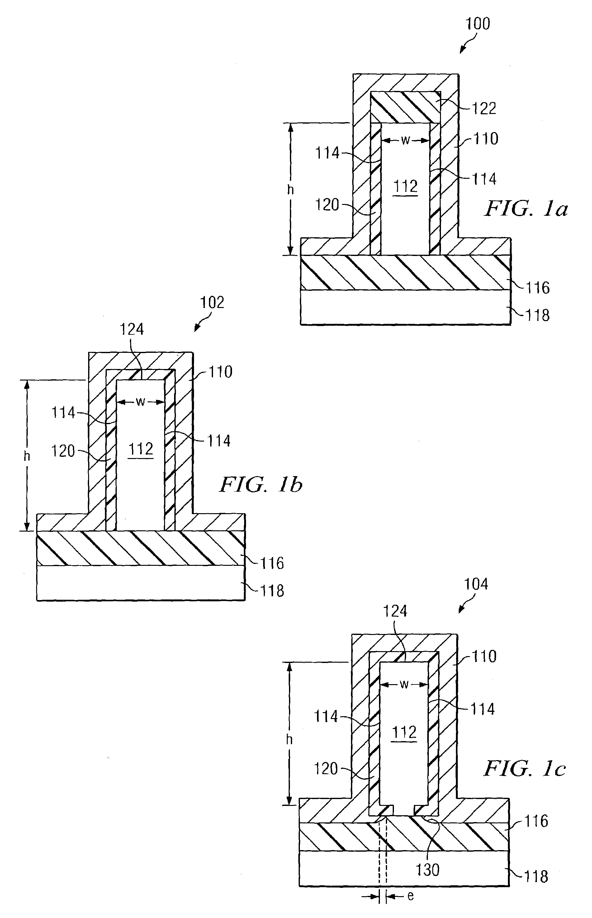
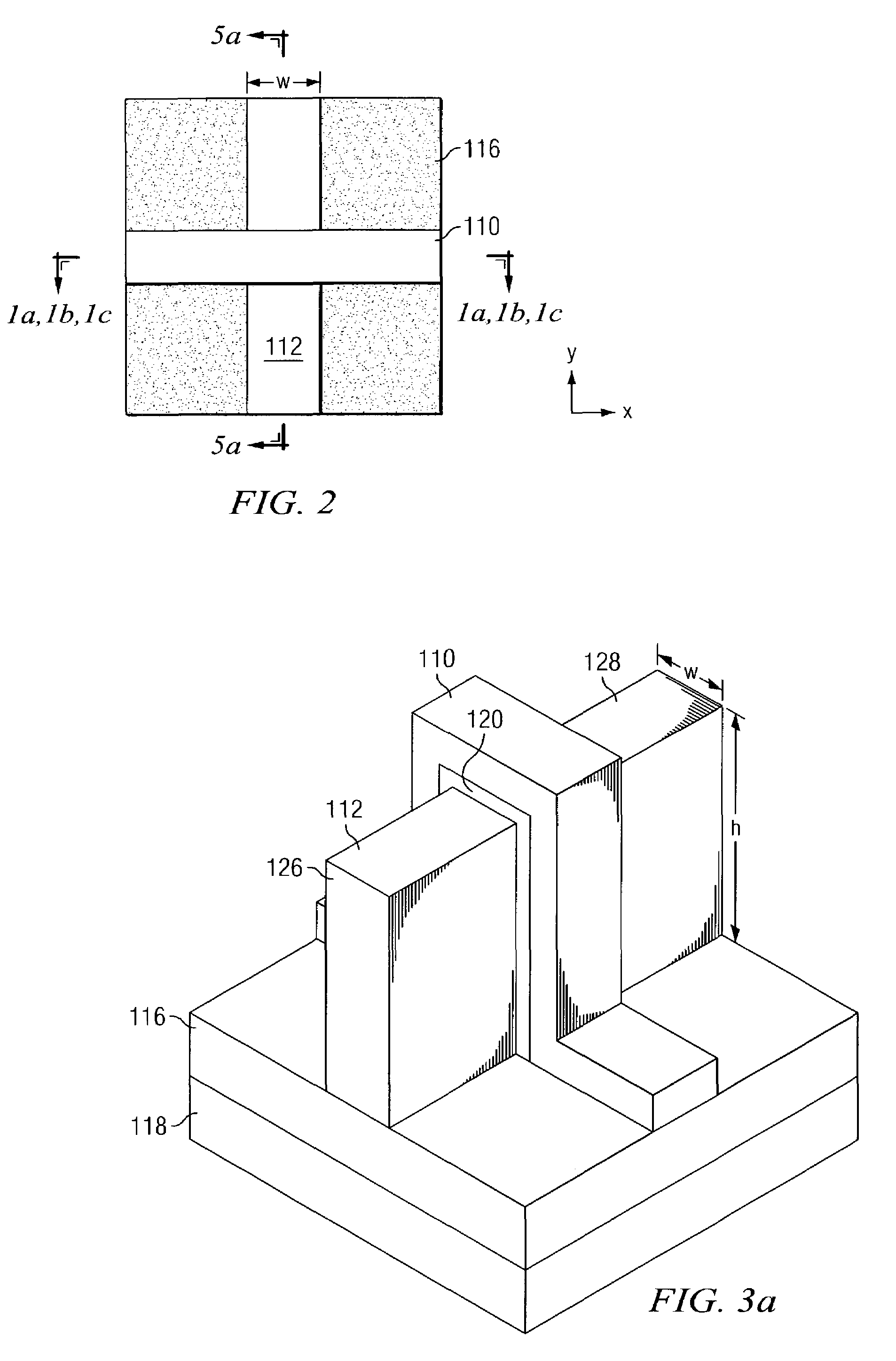
[0029]Another example of the multiple-gate transistor is the triple-gate transistor 102. The cross-section of the triple-gate transistor structure 102 is illustrated in FIG. 1b. The plan view of the triple-gate structure is the same as the double-gate structure and is shown in FIG. 2. The triple-gate transistor structure has a gate electrode 110 that forms three gates: one gate on the top surface 124 of the silicon body / fin 112, and two gates on the sidewalls 114 of the silicon body / fin 112. The triple-gate transistor achieves better gate control than the double-gate transistor because it has one more gate on the top of the silicon fin. A three-dimensional view of the triple-gate transistor 102 is shown in ...


PUM


Abstract

A semiconductor structure includes of a plurality of semiconductor fins overlying an insulator layer, a gate dielectric overlying a portion of said semiconductor fin, and a gate electrode overlying the gate dielectric. Each of the semiconductor fins has a top surface, a first sidewall surface, and a second sidewall surface. Dopant ions are implanted at a first angle (e.g., greater than about 7°) with respect to the normal of the top surface of the semiconductor fin to dope the first sidewall surface and the top surface. Further dopant ions are implanted with respect to the normal of the top surface of the semiconductor fin to dope the second sidewall surface and the top surface.

Description

TECHNICAL FIELD[0001]The present invention relates to semiconductor devices and more particularly to semiconductor devices with fin structures and methods for doping semiconductor fin devices.BACKGROUND[0002]The dominant semiconductor technology used for the manufacture of ultra-large scale integrated (ULSI) circuits is the metal-oxide-semiconductor field effect transistor (MOSFET) technology. Reduction in the size of MOSFETs has provided continued improvement in speed performance, circuit density, and cost per unit function over the past few decades. As the gate length of the conventional bulk MOSFET is reduced, the source and drain increasingly interact with the channel and gain influence on the channel potential. Consequently, a transistor with a short gate length suffers from problems related to the inability of the gate to substantially control the on and off states of the channel.[0003]Phenomena such as reduced gate control associated with transistors with short channel length...

Claims


Application Information

Patent Timeline
IPC IPC(8): H01L21/84H01L21/265H01L21/336H01L29/786
CPCH01L21/26586H01L29/785H01L29/66803
Inventor YEO, YEE-CHIAWANG, PING-WEICHEN, HAO-YUYANG, FU-LIANGHU, CHENMING
Owner TAIWAN SEMICON MFG CO LTD
Why Eureka
Try Eureka