Method for atomic layer deposition (ALD) of silicon oxide film

a silicon oxide film and atomic layer technology, applied in the direction of polycrystalline material growth, chemically reactive gas growth, crystal growth process, etc., can solve the problems of low deposition rate of thin film, deterioration of thin film properties, and inability to easily remove, so as to improve the deposition rate and high deposition rate

Inactive Publication Date: 2006-07-18
SAMSUNG ELECTRONICS CO LTD
View PDF29 Cites 151 Cited by
  • Summary
  • Abstract
  • Description
  • Claims
  • Application Information

AI Technical Summary

Benefits of technology

[0015]It is an object of the present invention to provide a method for forming a silicon oxide film at low temperature and a high deposition rate via an atomic layer deposition process.
[0016]In order to achieve the above-described object, the method for forming a silicon oxide film via an atomic layer deposition process employs a HCD source to improve the deposition rate instead of the conventional SiCl4 source.

Problems solved by technology

However, the conventional method requires high temperature of more than 600K, long time necessary for deposition and a large amount of sources.
First, when a silicon oxide film is deposited at a temperature ranging from room temperature to 50° C., the by-products from the reaction and unreacted liquid sources such as HCD and H2O are not easily removed due to low temperature in the reactor chamber. These materials exist as particles in the thin film after deposition, which deteriorate properties of the thin film.
Second, when a silicon oxide film is deposited at a temperature above 50° C., by-products resulting from reaction and unreacted liquid sources such as HCD and H2O are easily removed. However, the deposition rate of thin film is very low. That is, when a silicon oxide film is deposited using SiCl4, H2O and catalysts at a temperature above 50° C., the deposition rate is lower than 1.0 Å per cycle (see FIG. 1). As a result, the yield of device is reduced.
As a result, when a silicon oxide film is deposited via the atomic layer deposition process at low temperature below 400° C., in-situ cleaning cannot be performed.

Method used


Image

  • Method for atomic layer deposition (ALD) of silicon oxide film
  • Method for atomic layer deposition (ALD) of silicon oxide film
  • Method for atomic layer deposition (ALD) of silicon oxide film

Examples


example 1

Variation in Deposition Rate of Silicon Oxide Film Depending on Increase in Amount of HCD Source

[0045]The following experiment was conducted to find out the deposition rate of silicon oxide film depending on the increase in the amount of HCD source. HCD where the flow rate varies as shown in FIG. 4 and pyridine having a flow rate of 100 sccm were provided to a chamber. Residual sources in the chamber were then removed by pumping until the pressure reaches 1 mTorr. Thereafter, H2O having a flow rate of 500 sccm and pyridine having a flow rate of 100 sccm were provided to the chamber, and the residual sources were again removed by pumping until the pressure reaches 1 mTorr. Above processes were repeated to form a silicon oxide film.

[0046]As shown in FIG. 4, the deposition rate increased as the amount of HCD source increased. The deposition rate was saturated at 2 Å / cycle. The saturation occurs due to self-limiting condition of HCD and chemical species adsorbed to the surface of the su...

example 2

Variation of Deposition Rate of Silicon Oxide Film Depending on Deposition Temperature

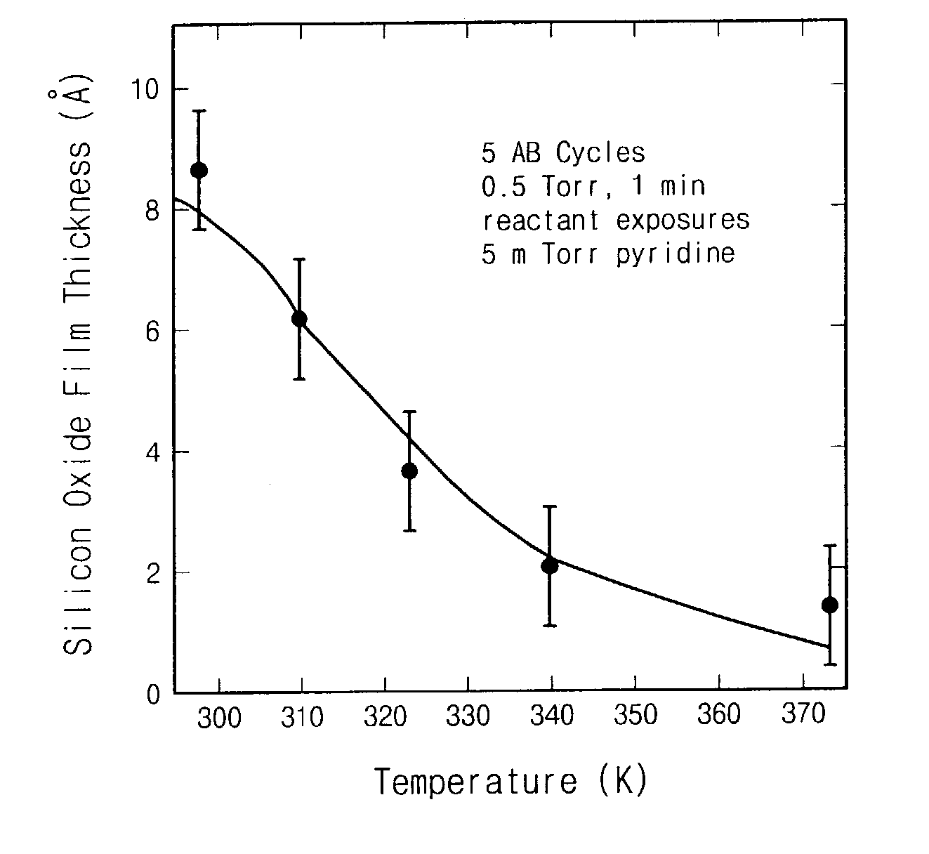
[0047]The following experiment was conducted to find out the deposition rate of silicon oxide film depending on deposition temperature. For the comparison with U.S. Pat. No. 6,090,422 wherein SiCl4 is used, the experiment was conducted at the temperature similar to that of U.S. Pat. No. 6,090,422 shown in FIG. 1. HCD having a flow rate of 500 sccm and pyridine having a flow rate of 100 sccm were provided to a chamber. Residual sources in the chamber were then removed by pumping until the pressure reaches 1 mTorr. Thereafter, H2O having a flow rate of 500 sccm and pyridine having a flow rate of 100 sccm were provided to the chamber, and the residual sources were again removed by pumping until the pressure reaches 1 mTorr. Above processes were repeated to form a silicon oxide film.

[0048]As shown in FIG. 5, the deposition rate of silicon oxide film decreased as the deposition temperature increased. Ho...


PUM

PropertyMeasurementUnit
temperatureaaaaaaaaaa

Abstract

The present invention relates to a method for forming silicon oxide films on substrates using an atomic layer deposition process. Specifically, the silicon oxide films are formed at low temperature and high deposition rate via the atomic layer deposition process using a Si2Cl6 source unlike a conventional atomic layer deposition process using a SiCl4 source. The atomic layer deposition apparatus used in the above process can be in-situ cleaned effectively at low temperature using a HF gas or a mixture gas of HF gas and gas containing —OH group.

Description

BACKGROUND OF THE INVENTION[0001]1. Field of the Invention[0002]The present invention generally relates to methods for forming silicon oxide films on substrates via atomic layer deposition (hereinafter, referred to as ‘ALD’) processes, and more specifically, to a method for forming a silicon oxide film at low temperature and high deposition rate using Si2Cl6 (hexachloro disilane; hereinafter, referred to as ‘HCD’) and H2O sources, and catalysts.[0003]2. Description of the Prior Art[0004]Generally, a silicon oxide film is one of the most commonly used thin films in a semiconductor since it provides superior interface with silicon and has excellent dielectric characteristics. There are two conventional methods for depositing a silicon oxide film: (1) oxidation process wherein silicon is oxidized at a temperature of more than 1000° C.; and (2) a Chemical Vapor Deposition (CVD) process wherein more than two sources are provided at a temperature ranging from 600 to 800° C. These methods ...

Claims


Application Information

Patent Timeline
Patent Type & Authority Patents(United States)
IPC IPC(8): C30B23/00C23C16/40C23C16/44C23C16/455C30B25/14C30B29/18
CPCC23C16/402C23C16/4405C30B29/18C23C16/45534C30B25/14C23C16/45531C23C16/40
Inventor CHO, BYOUNG HAKIM, YONG ILSHIN, CHEOL HOLEE, WON HYUNGKIM, JUNG SOOSIM, SANG TAE
Owner SAMSUNG ELECTRONICS CO LTD
Why Eureka
Try Eureka