
Multi-threshold-voltage integrated circuit having a non-volatile data storage circuit

a data storage circuit and multi-threshold voltage technology, applied in the field of integrated circuits, can solve the problems of increasing power consumption, volatile data held in latches and flip-flops inside the circuit, and not being suited to automatic layout, so as to achieve a higher degree of precision

Active Publication Date: 2006-07-18
FUJITSU SEMICON LTD
View PDF5 Cites 29 Cited by
  • Summary
  • Abstract
  • Description
  • Claims
  • Application Information

AI Technical Summary

Benefits of technology

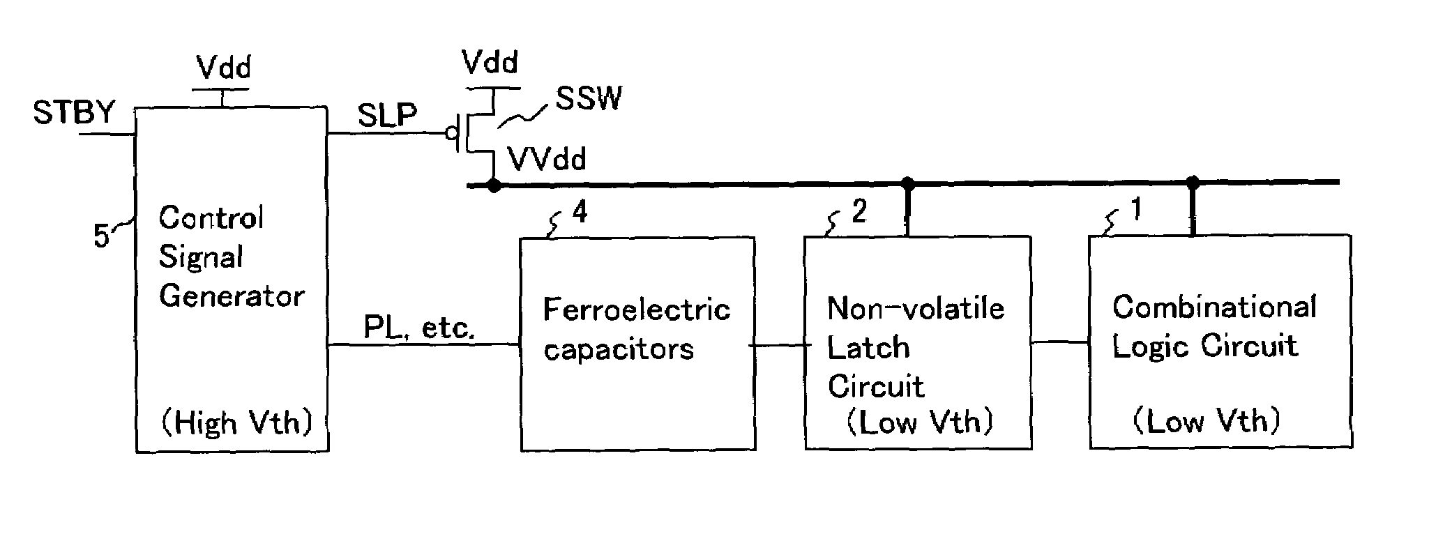
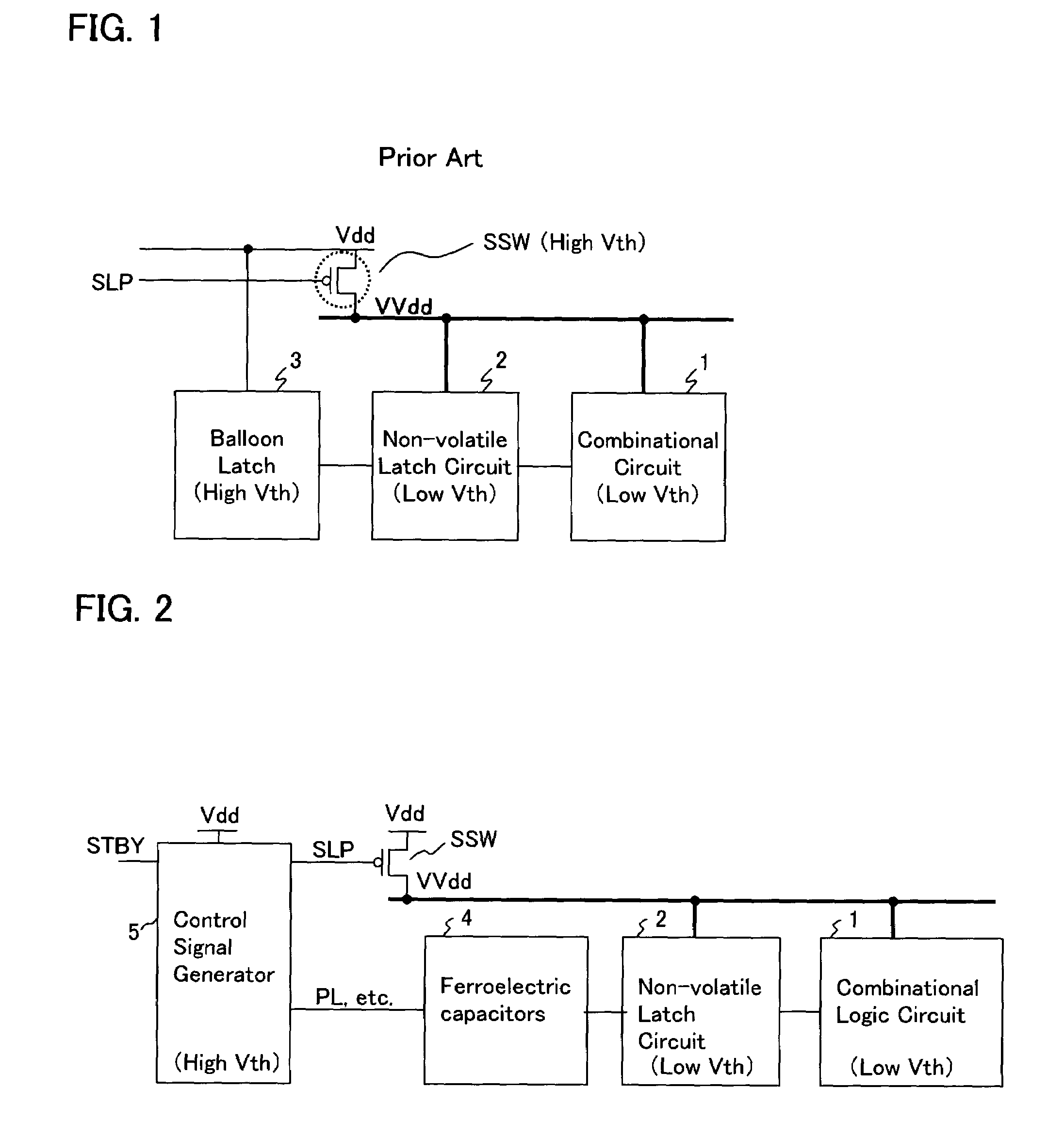
[0018]According to this first aspect of the present invention, a ferroelectric capacitor for holding data held by a nonvolatile latch circuit during sleep mode is provided in an integrated circuit constructed using MTCMOS technology, and a sleep switch for switching the power supply off during sleep mode is used as an activation circuit for activating the latch circuit when recovering from sleep mode. More specifically, at a timing when the other ferroelectric capacitor terminal is driven to produce voltages in the pair of terminals of the latch circuit, the sleep switch is caused to conduct, thereby activating the latch signal, and data pertaining to the difference between these voltages are then latched. As a result, the latch circuit can securely restore the data. Further, since there is no need to connect the first power line to the ferroelectric capacitor, the power line layout is simplified. Since the ferroelectric capacitor does not require a high-Vth transistor, the circuit element area can be reduced. Only the sleep switch is constituted by a high-Vth transistor, and therefore the number of transistors with high-Vth may be reduced.
[0022]In a preferable embodiment of this aspect of the invention, the ferroelectric capacitor comprises two pairs of ferroelectric capacitors, one terminal of each ferroelectric capacitor being connected to the pair of storage terminals of the latch circuit. The other terminals of one of the ferroelectric capacitors of the ferroelectric capacitor pair connected to each storage terminal of the latch circuit are driven by the plate signal. As a result of this driving, a voltage difference in accordance with the polarization directions of the ferroelectric capacitor pair connected to each storage terminal is generated in the pair of storage terminals of the latch circuit. By providing a ferroelectric capacitor pair for each of the storage terminals of the latch circuit, the difference between the voltages generated by the driving performed by the plate signal increases, whereby a data recall operation can be performed with a higher degree of precision.

Problems solved by technology

In the low-Vth transistor, however, leakage current is generated during standby period or sleep mode period (to be referred to as “sleep mode” hereinafter), leading to an increase in power consumption.
Since no power supply voltage is supplied, however, a problem arises in that the data held in the latches and flip-flops inside the circuit become volatile.
In the MTCMOS circuit having a balloon-type data holding circuit illustrated in FIG. 1, however, the normal power line Vdd and virtual power line VVdd are mixed together, and therefore this example is not suited to an automatic layout.
As a result, the normal power line Vdd and virtual power line VVdd become mixed together over the entire chip, which complicates the layout and is therefore disadvantageous as regards the degree of integration.
As a result, transistors of differing threshold voltages are mixed together, and since it is necessary to keep a sufficient distance on the chip between these transistors due to structural differences, a problem arises in that the degree of integration deteriorates.
When the power is switched on again in the nonvolatile latch circuit employed in the nonvolatile SRAM of non-patent document 2, however, a problem arises in that the data to be recovered tend to invert due to irregularities in the transistor characteristic of the latch circuit.
The latch circuit in this prior application, however, does not employ MTCMOS technology.

Method used


Image

  • Multi-threshold-voltage integrated circuit having a non-volatile data storage circuit
  • Multi-threshold-voltage integrated circuit having a non-volatile data storage circuit
  • Multi-threshold-voltage integrated circuit having a non-volatile data storage circuit

Examples


Embodiment Construction

[0043]An embodiment of the present invention will be described below with reference to the drawings. However, the scope of protection of the present invention is not limited to or by the following embodiment, but covers the inventions described in the patent claims and equivalent items thereto.

[0044]FIG. 2 is a schematic constitutional diagram of an integrated circuit in this embodiment. Similarly to the example in FIG. 1, a normal power supply Vdd and a virtual power supply VVdd are connected via a sleep switch SSW, and a combinational logic circuit 1 and nonvolatile latch circuit 2 are connected to the virtual power supply VVdd. The sleep switch SSW is constituted by a high-Vth transistor, whereas the combinational logic circuit 1 and nonvolatile latch circuit 2 are constituted by low-Vth transistors.

[0045]The integrated circuit of this embodiment is provided with a ferroelectric capacitor 4 for holding the data held in the nonvolatile latch circuit 2 even when the sleep switch SS...


PUM


Abstract

An integrated circuit has a sleep switch, provided between a first power line and a second power line, which is constituted by a transistor of a first threshold voltage, and which becomes non-conducting in a sleep mode, and further has a latch circuit, connected to the second power line, which is constituted by a transistor of a second threshold voltage which is lower than the first threshold voltage, and a ferroelectric capacitor for storing data held in the latch circuit in accordance with the polarization direction of a ferroelectric film thereof. The integrated circuit also comprises a control signal generating circuit which, when returning to an active mode from the sleep mode, generates a plate signal for driving a terminal of the ferroelectric capacitor to generate a voltage in the latch circuit in accordance with the polarization direction, and generates a sleep signal for causing the sleep switch to conduct to thereby activate the latch circuit following the driving of the ferroelectric capacitor.

Description

CROSS-REFERENCE TO RELATED APPLICATIONS[0001]This application is based upon and claims the benefit of priority from the prior Japanese Patent Application No. 2002-247346, filed on Aug. 27, 2002, the entire contents of which are incorporated herein by reference.BACKGROUND OF THE INVENTION[0002]1. Field of the Invention[0003]The present invention relates to an integrated circuit provided with a nonvolatile data storage circuit in a multi-threshold-voltage CMOS for enabling low power consumption, and more particularly to an integrated circuit which is capable of simplifying a power supply layout and avoiding erroneous operations during a data recall operation.[0004]2. Description of the Related Art[0005]A multi-threshold-voltage CMOS (MTCMOS) has been proposed as technology for reducing power consumption in an LSI (large-scale integrated circuit). According to this MTCMOS technology, as described in non-patent document 1, for example, which will be described herein below, the high curr...

Claims


Application Information

Patent Timeline
IPC IPC(8): G06F1/32G11C11/22H01L21/822G11C14/00G11C16/34H01L21/82H01L27/04H03K19/00H03K19/173H03K19/185
CPCG11C14/00G11C14/0072G11C16/34
Inventor YOKOZEKI, WATARUMASUI, SHOICHI
Owner FUJITSU SEMICON LTD
Learn More