[0022]The exemplary embodiments of the present invention may provide a semiconductor IC device having high reliability, by alleviating warping of an interlayer insulating film so as to prevent
cracking a protective film on application of stress on a protruded
electrode in packaging (in bonding) in order to prevent failure such as electrical disconnection and the like.
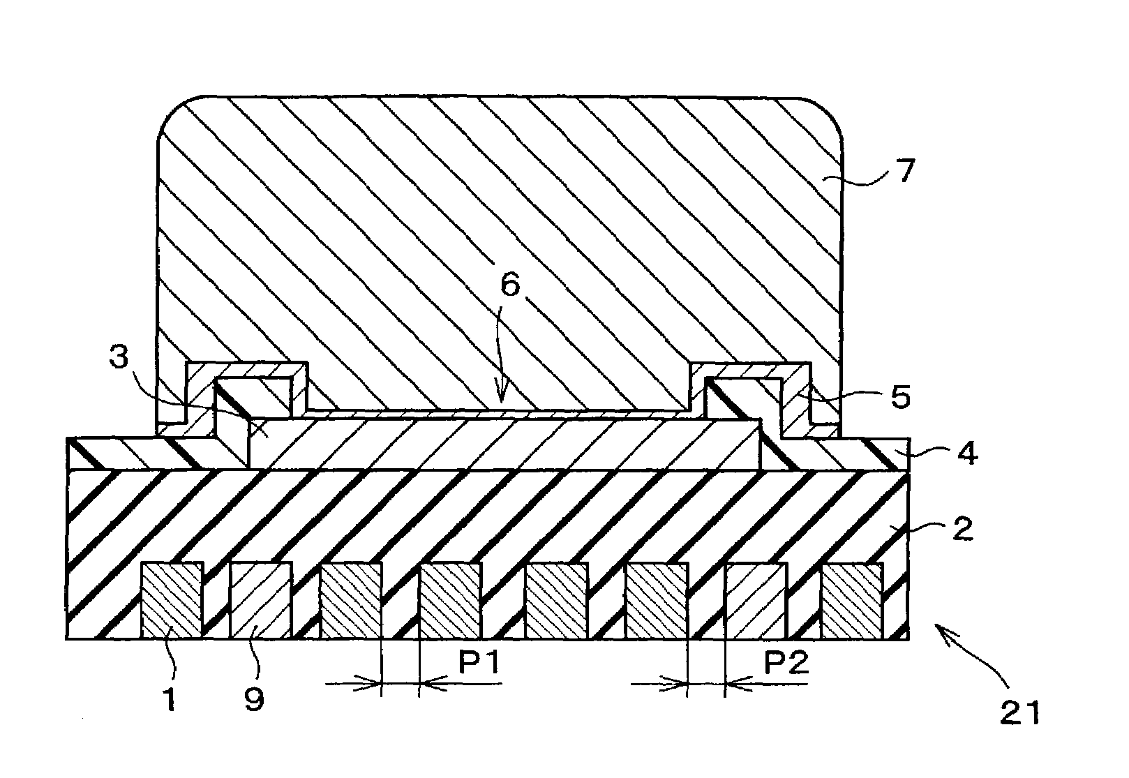
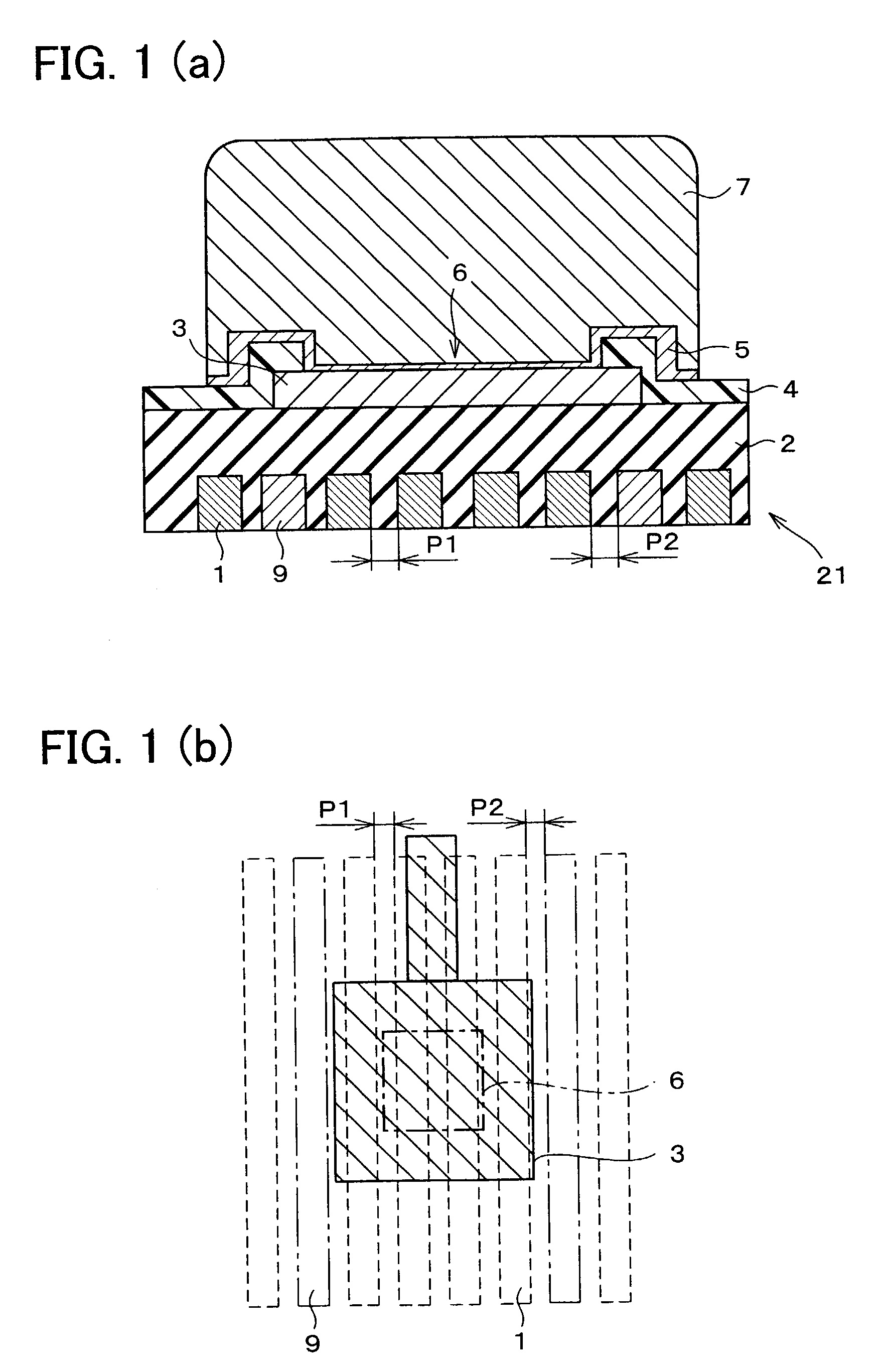
[0023]In order to solve the foregoing problems, a semiconductor integrated circuit device of the present invention includes (i) a first wiring layer in which a plurality of wires electrically connected with an operation area are aligned, (ii) a second wiring layer formed on an interlayer insulating film with which the first wiring layer is coated, and (iii) protruded electrodes provided on the second wiring layer, the protruded electrodes being so formed as to at least partially overlap the operation area, and being for establishing external
electrical connection, wherein the wires right under the protruded electrodes are so aligned as to have such pitches as to prevent warping of the interlayer insulating film due to pressure application in connecting the protruded electrodes with external connecting terminals.
[0026]However, the semiconductor IC device of the present invention has substantially narrow pitches between wires right under the protruded electrodes, because right under the protruded electrodes, a substantial pressure is applied in connecting the protruded electrodes with the external connective terminals. This arrangement may prevent the warping of the interlayer insulating film. For example, it is so arranged that the pitches between wires of the first wiring layer (inter-wire spaces) may be narrower than conventional pitches between wires. This arrangement may increases volume (total amount) of the first wiring layer compared with the interlayer insulating film around the first wiring layer, which is provided in the interlayer insulating film, thereby reducing a volumetric ratio of the interlayer insulating film around the first wiring layer to the first wiring layer, as compared with the volumetric ratio of the conventional interlayer insulating film. In short, by having narrower inter-wire spaces in the first wiring layer, the amount (total amount) of the interlayer insulating film is decreased around the first wiring layer, which is provided in the interlayer insulating film.
[0027]Therefore, for example, it is possible to reduce the volumetric ratio of the soft material in the area in which wires of the first wiring layer are provided with such narrow pitches. Thus, the warping of the interlayer insulating film of the semiconductor IC device is smaller than that of the conventional interlayer insulating film. As a result, for example, stress due to the warping of the interlayer insulating film, and like will not be applied on the protective film and the like provided on the interlayer insulating film. This prevents occurrence of a crack and the like in the protective film. Therefore, it is possible to prevent failure such as electrical disconnection in the second wring layer due to the crack and the like in the protective film, thereby giving high reliability to the semiconductor IC device of the present invention.
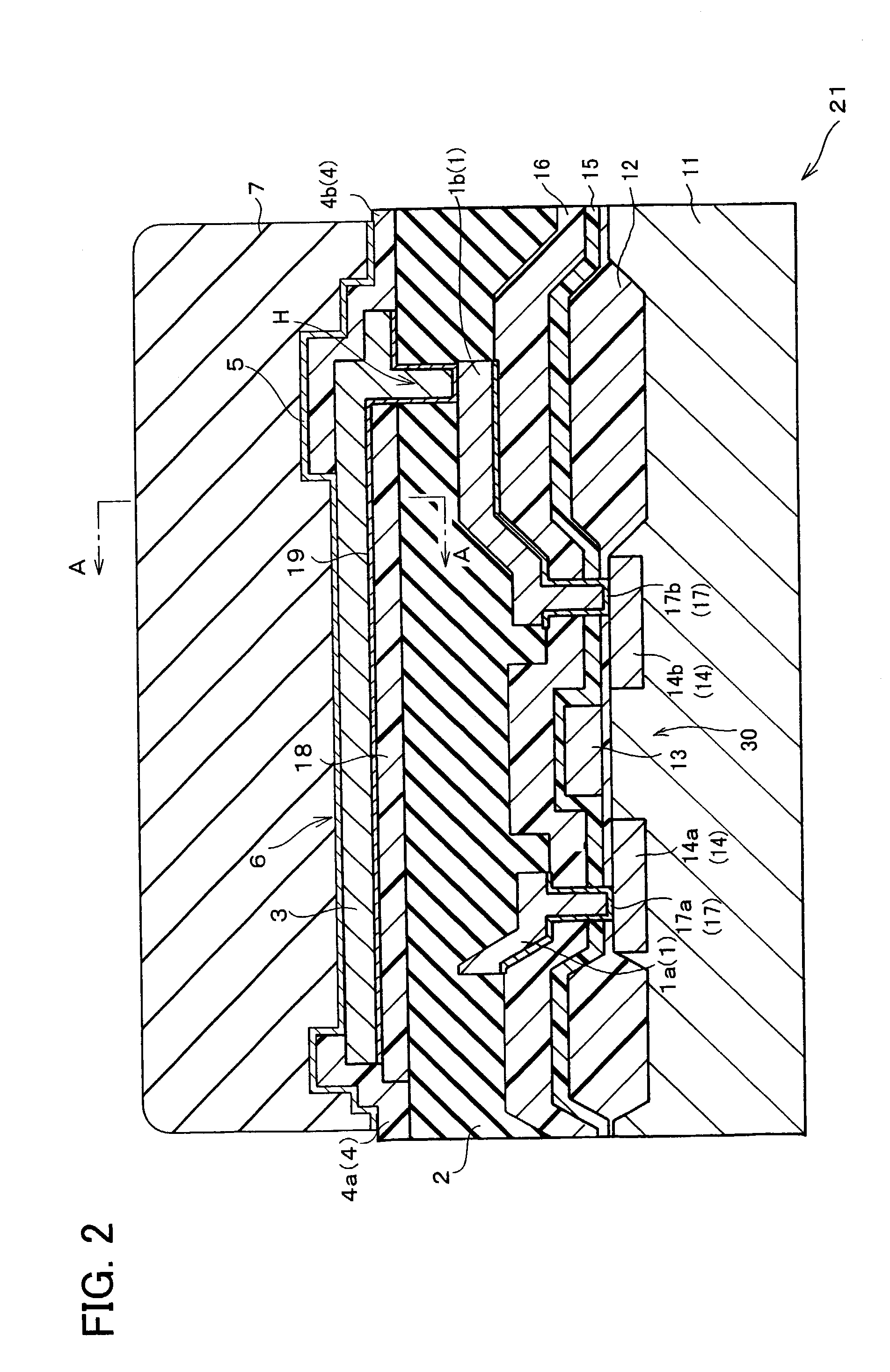
[0029]In this arrangement, the pseudo wires electrically disconnected with the operation area are respectively provided right under the protruded electrodes, because right under the protruded electrodes, a large pressure is especially applied in connecting the protruded electrodes with the external connective terminals. Thus, the warping of the interlayer insulating film of the semiconductor IC device is smaller than that of the conventional interlayer insulating film. As a result, for example, stress due to the warping of the interlayer insulating film, and like will not be applied on the protective film and the like provided on the interlayer insulating film. This prevents occurrence of a crack and the like in the protective film. Therefore, it is possible to prevent failure such as electrical disconnection in the second wring layer due to the crack and the like in the protective film.

