Annealing furnace, manufacturing apparatus, annealing method and manufacturing method of electronic device
a technology of electronic devices and manufacturing equipment, applied in the direction of coatings, transistors, chemical vapor deposition coatings, etc., can solve the problems of inferior electrical characteristics, difficult to form ultra thin insulating films with a thickness of 2 nm or less with great repeatability, and native oxide films formed on the surface of si substrates
- Summary
- Abstract
- Description
- Claims
- Application Information
AI Technical Summary
Benefits of technology
Problems solved by technology
Method used
Image
Examples
first embodiment
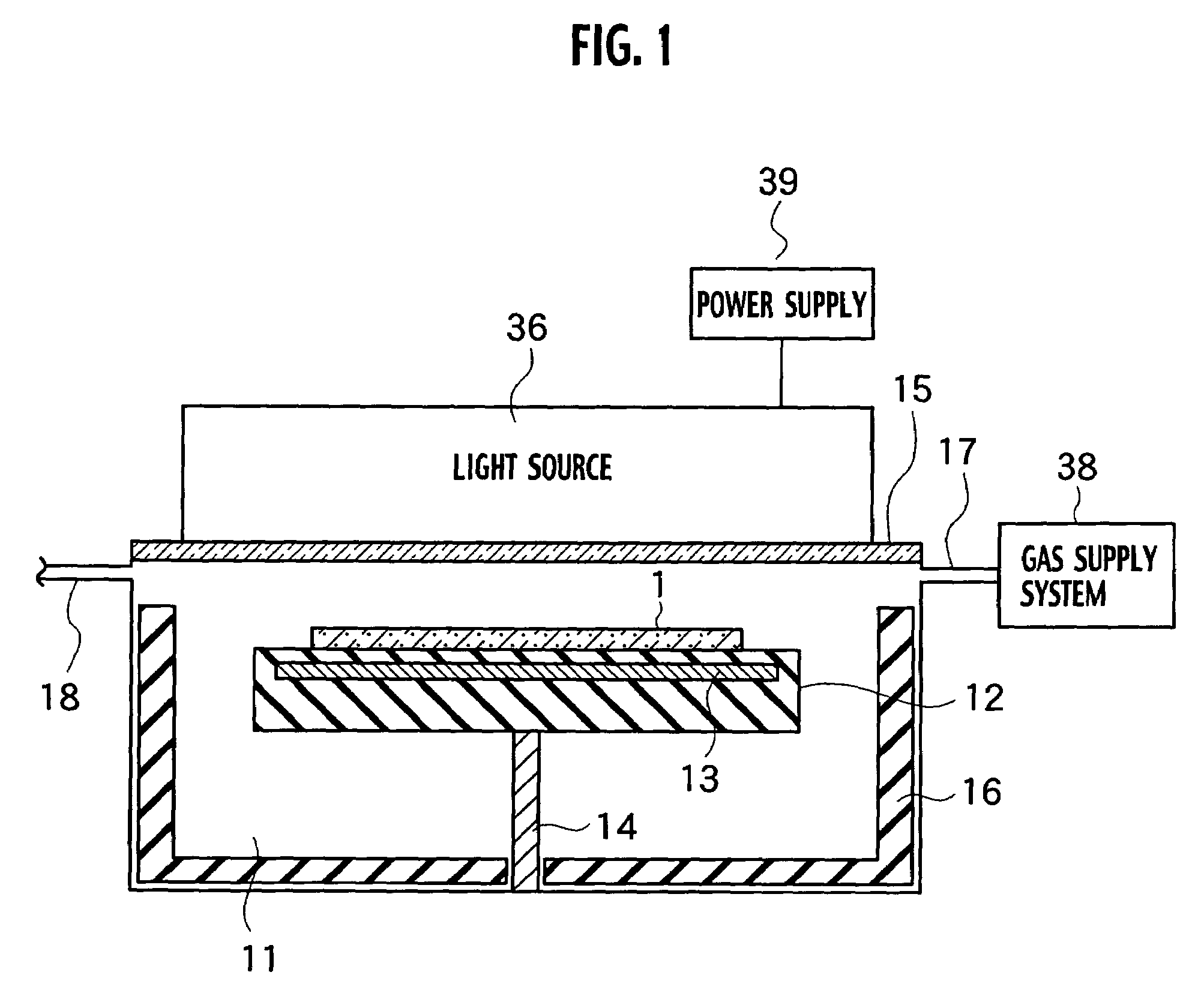
[0034]As shown in FIG. 1, an annealing furnace according to a first embodiment of the present invention includes a processing chamber 11, a susceptor 12, an introduction conduit 17, an exhaust conduit 18, a transparent window 15 and a main heater 36. Herein, a substrate 1 such as a semiconductor substrate is processed in the processing chamber 11. The susceptor 12, on which the substrate 1 is loaded, is located in the processing chamber 11. The introduction conduit 17 supplies gas in parallel to the surface of the substrate 1. The exhaust conduit 18 exhausts gas from the processing chamber 11. The transparent window 15 is located facing the susceptor 12 on the top of the processing chamber 11. The main heater 36 irradiates the surface of the substrate 1 from the transparent window 15 with pulsed light.
[0035]The processing chamber 11 is made of a metal such as stainless steel. The susceptor 12, on which the substrate 1 is loaded, is located on the top of a support shaft 14 installed ...
second embodiment
[0044]As shown in FIG. 6, in a manufacturing apparatus according to a second embodiment of the present invention, first and second processing apparatuses 21 and 22 are connected to a transfer chamber 30 through gate valves 34a and 34b, respectively. The first processing apparatus 21 has a first processing chamber 11a in which a first susceptor 12a is located, and a substrate 1 is loaded on the first susceptor 12a. The second processing apparatus 22 has a second processing chamber 11b in which a second susceptor 12b is located, and a substrate 1a is loaded on the second susceptor 12b. To the first and second processing chambers 11a and 11b, first and second introduction conduits 17a and 17b are connected to supply a variety of gases from a gas supply system 38. To the transfer chamber 30, first and second cassette chambers 10 and 20 are installed. In the first cassette chamber 10, a wafer cassette storing the substrates 1 and 1a is placed. In the second cassette chamber 20, a wafer c...
third embodiment
[0071]As shown in FIG. 19, a manufacturing apparatus according to a third embodiment of the present invention includes first and second processing apparatuses 21a and 22a. In the second embodiment, the first and second processing apparatuses 21 and 22 are both used to form the insulting film. The third embodiment differs from the second embodiment in that a pretreatment of removing a native oxide film on the surface of a substrate 1 is performed in the first processing apparatus 21a, and a processing of forming an insulating film is performed in the second processing apparatus 22a. Other than that, the third embodiment is the same as the second embodiment. Thus, redundant descriptions will be omitted.
[0072]In the first processing apparatus 21a, pretreatment gas for removing a native oxide film on the surface of a substrate 1 loaded on a first susceptor 12a is supplied from a gas supply system 38. For pretreatment gas, reduction gas such as H2 gas, mixed gas containing H2, compound g...
PUM
| Property | Measurement | Unit |
|---|---|---|
| temperature | aaaaa | aaaaa |
| temperature | aaaaa | aaaaa |
| thickness | aaaaa | aaaaa |
Abstract
Description
Claims
Application Information


