Low temperature process for passivation applications

a low temperature process and application technology, applied in the manufacture of cold cathode, electric discharge tube/lamp, electrolyte system, etc., can solve the problems of unsatisfactory encapsulation technique and unsatisfactory three-layer protective covering described by haskal et al., and achieve improved encapsulation properties, low etching rate, good adhesion properties

Inactive Publication Date: 2006-08-08
APPLIED MATERIALS INC
View PDF25 Cites 35 Cited by
  • Summary
  • Abstract
  • Description
  • Claims
  • Application Information

AI Technical Summary

Benefits of technology

[0013]The present invention provides organic electroluminescent devices that have improved encapsulation properties. The present invention further provides improved methods for encapsulating such devices. In some embodiments of the present invention, a multilayer encapsulation approach is taken. In some embodiments, each encapsulation layer has the same properties. In other embodiments, the first encapsulation layer is optimized for adhesion to an electrode layer in the device. Subsequent encapsulation layers help protect the device from environmental elements such as moisture. In some embodiments, the first (inner) encapsulation layer is a silicon rich silicon nitride film while one or more outer encapsulation layers are silicon nitride films that have low etch rates. The silicon rich silicon nitride films of the present invention have good adhesion properties. Further, the present invention provides a method for improving adhesion to the cathode layer of electroluminescent devices.
[0014]Silicon nitride deposition is typically performed in a PECVD chamber at temperatures that would cause damage to the organic layers of the electroluminescent device. However, using the techniques of the present invention, electroluminescent devices are encapsulated using PECVD or related techniques without damaging the organic layers of the electroluminescent device. This is achieved, in part, by cycling the deposition process between an active deposition state and an inactive cooling state. The inactive cooling state allows the device substrate to cool so that the integrity of the organic layer of the device is not lost.

Problems solved by technology

Such an encapsulation technique is unsatisfactory.
The three-layer protective covering described by Haskal et al. is unsatisfactory, however, because it is time consuming to manufacture the coverings described by Haskal et al.

Method used


Image

  • Low temperature process for passivation applications
  • Low temperature process for passivation applications
  • Low temperature process for passivation applications

Examples


Embodiment Construction

[0025]The present invention provides methods for encapsulating electroluminescent devices in order to protect them from elements like moisture. Further, the present invention provides methods for improving adhesion to the cathode layer of electroluminescent devices. In particular, the cathode layer is subjected to an H2 plasma for a period of time prior to deposition of materials onto the cathode layer in order to complete the electroluminescent device. Representative electroluminescent devices include organic light-emitting diodes (OLEDs) and polymer light-emitting diodes. Typically, the electroluminescent device is used in devices such as car radios, mobile phones, digital cameras, camcorders, and personal digital assistants.

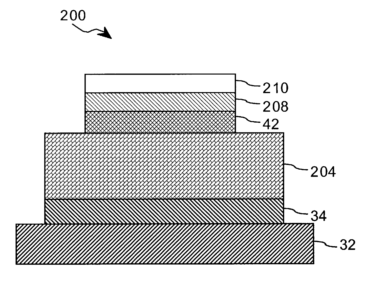
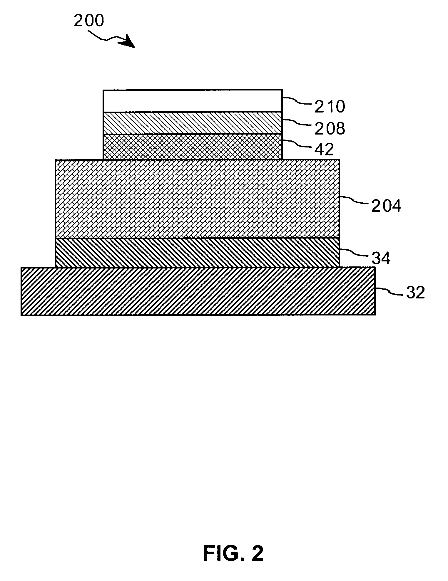
[0026]A typical electroluminescent device (e.g., OLED) in accordance with the present invention is illustrated in FIG. 2. The electroluminescent device 200 comprises a substrate 32, an anode 34 on substrate 32, an organic layer 204, a cathode layer 42 on organ...


PUM


Abstract

An organic electroluminescent device comprising an anode layer on a substrate, an organic layer on the anode layer, and a cathode layer on the organic layer. In one embodiment, the cathode layer is subjected to H2 plasma prior to deposition of a protective layer over the cathode. In another embodiment, the organic electroluminescent device is encapsulated with an inner encapsulation layer on the cathode layer, and an outer encapsulation layer on the inner encapsulation layer. The inner layer is optimized for adhesion to the cathode layer.

Description

1. FIELD OF THE INVENTION[0001]The present invention relates to improved organic electroluminescent devices and improved methods for manufacturing organic electroluminescent devices. Organic electroluminescent devices include organic light-emitting diodes and polymer light-emitting diodes. They are used in a number of devices, such as car radios, mobile phones, digital cameras, camcorders, and personal digital assistants.2. BACKGROUND OF THE INVENTION[0002]Over the past two decades, new flat panel display technology based on light emission from thin layers of small organic molecules (organic light-emitting diodes or OLEDs) or conducting polymers (polymer light-emitting diodes or PLEDs) has emerged. Compared to liquid crystal-based displays (LCDs), this technology offers higher contrast displays with lower power consumption, and response times fast enough for video applications. Displays based on OLED and PLED technology exhibit a much wider viewing angle than liquid crystal displays...

Claims


Application Information

Patent Timeline
Patent Type & Authority Patents(United States)
IPC IPC(8): H01J9/00H01J9/24H01L51/52
CPCH01L51/5237H10K50/844H10K50/84H10K77/10H01L21/02142H01L21/02274
Inventor HSIAO, MARKTAKEHARA, TAKAKOSHANG, QUANYUANHARSHBARGER, WILLIAM R.
Owner APPLIED MATERIALS INC
Why Eureka
Try Eureka