Method for producing a structure using nanoparticles

a technology of nanoparticles and nanoparticles, applied in the direction of printed circuits, printed circuit manufacturing, conductive pattern formation, etc., can solve the problem of reducing the temperature increase, and achieve the effect of simple and efficien

Inactive Publication Date: 2006-08-08
RGT UNIV OF CALIFORNIA +1
View PDF10 Cites 30 Cited by
  • Summary
  • Abstract
  • Description
  • Claims
  • Application Information

AI Technical Summary

Benefits of technology

[0007]Hence, it is a general object of the invention to provide a device and method for preparing fine structures using nanoparticles that is simple and efficient.
[0009]Accordingly, in some embodiments the nanoparticles are applied in drops of a suspension to the substrate using a droplet generator, which reduces the amount of suspension required. The particles are molten at least in part by exposing to laser light, whereupon they are solidified, thus forming a solid structure in those places where the nanoparticles where heated by the laser. This provides an efficient, low-loss method for forming a structure on the substrate. Compared to the method of heating the nanoparticles on the substrate in an oven or on a hotplate, laser curing leads to local heating only, so that damage to thermally sensitive regions in other areas of the substrate can be avoided. This is particularly important in the formation of conductive interconnections in integrated circuits in which thermal damage to other regions of the circuit may occur if heat applied to the nanoparticles is widely dispersed. In addition, the laser light is at least partially absorbed by the particles directly and not by the substrate, which also tends to reduce the temperature increase in the latter.
[0010]The laser light may have non-Gaussian intensity distribution for optimizing the quality of the generated structure, or it may be pulsed for improved control of the heat flow into the substrate.

Problems solved by technology

In addition, the laser light is at least partially absorbed by the particles directly and not by the substrate, which also tends to reduce the temperature increase in the latter.

Method used


Image

  • Method for producing a structure using nanoparticles
  • Method for producing a structure using nanoparticles
  • Method for producing a structure using nanoparticles

Examples


example 1

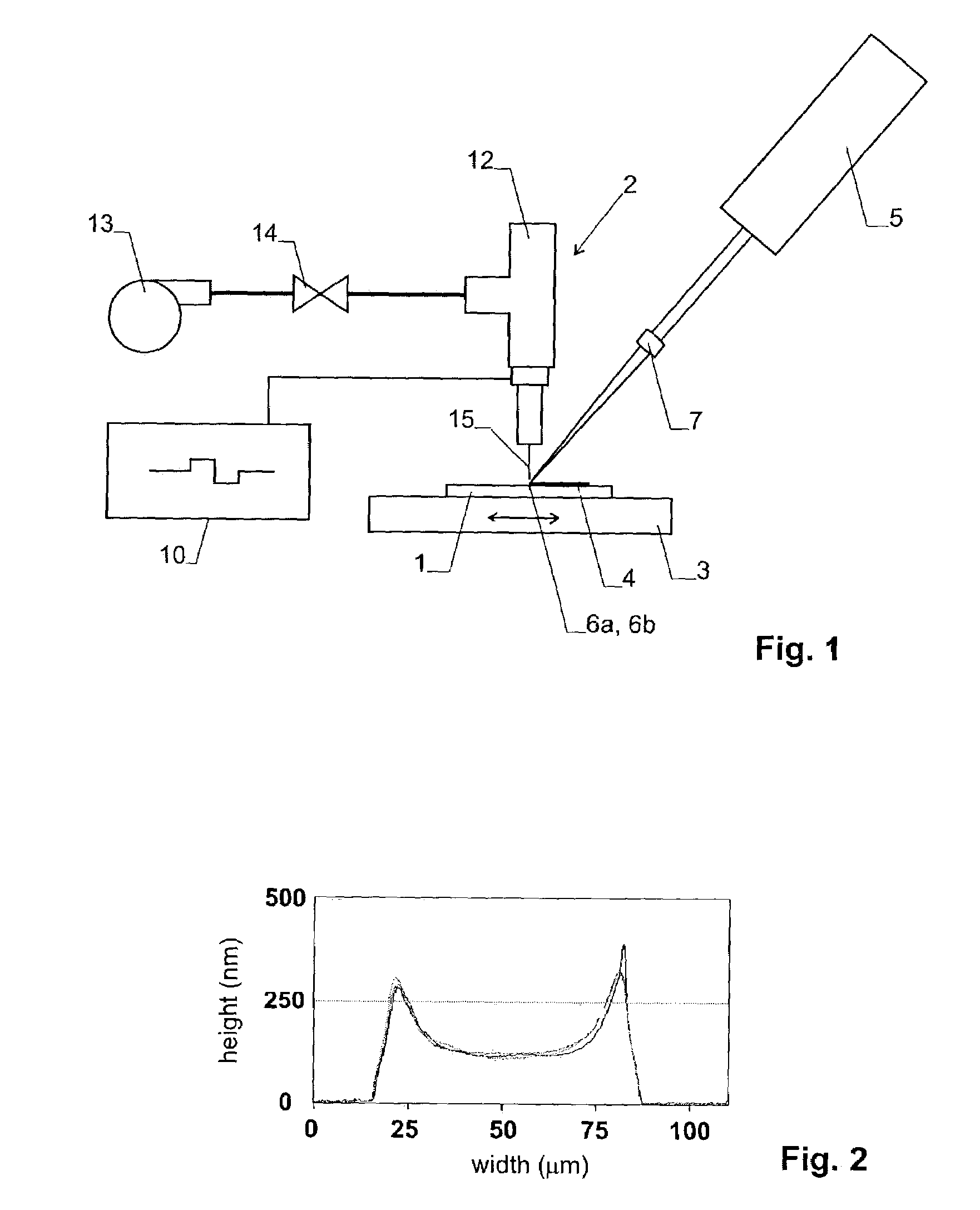
[0055]In a first example, gold nanoparticles with a mean average size of approximately 2 to 5 nm were suspended in toluene. The mass-fraction of gold in the solution was approximately 40% of the total weight.

[0056]Droplets were generated with a drop-on-demand piezoelectric jetting device as mentioned above.

[0057]The drops 3 were deposited to form printed line strip 4 on a silicon wafer substrate by moving the substrate continuously at a speed of 1 mm / s with a positioning stage. Printed line strip 4 was simultaneously cured by light from an argon ion laser at a wavelength of 488 nm, where the suspension had an absorption of less than 1 μm−1. The curing point 6b was located right behind the point 6a where the drops impinged on the substrate 1. It had a diameter of approximately 100 μm.

[0058]After cooling, the remaining structure consisted of solid, continuous, electrically conducting gold lines with good electrical conductance. The lines had a typical width of approximately 60–100 μm....

example 2

[0059]In a second example, the gold in toluene suspension as mentioned under “nanoparticles, suspension” above has been used. Droplets of approximately 46 μm diameter were applied at a rate of 30 Hz to a glass substrate moving at 2 mm / s. The width of the deposited (still liquid) line was measured to be about 125 μm.

[0060]After printing, a continuous cw-Argon laser beam at 514 nm was applied for curing with the same translation speed of 2 mm / s to the center of the printed line at an angle of incidence of 45°. The laser beam had a power of 100 mW and the beam waist (1 / e2) was 27 μm.

[0061]Atomic force microscope (AFM) images were recorded for evaluating the cross section of the cured printed line. A thickness profile along three different lines perpendicular to the printed line are shown in FIG. 2. As can be seen, the cured line strip has a maximum thickness at its edges. The non-uniformity of the thickness is attributed to thermal diffusion of gold particles towards the edge of the be...

example 3

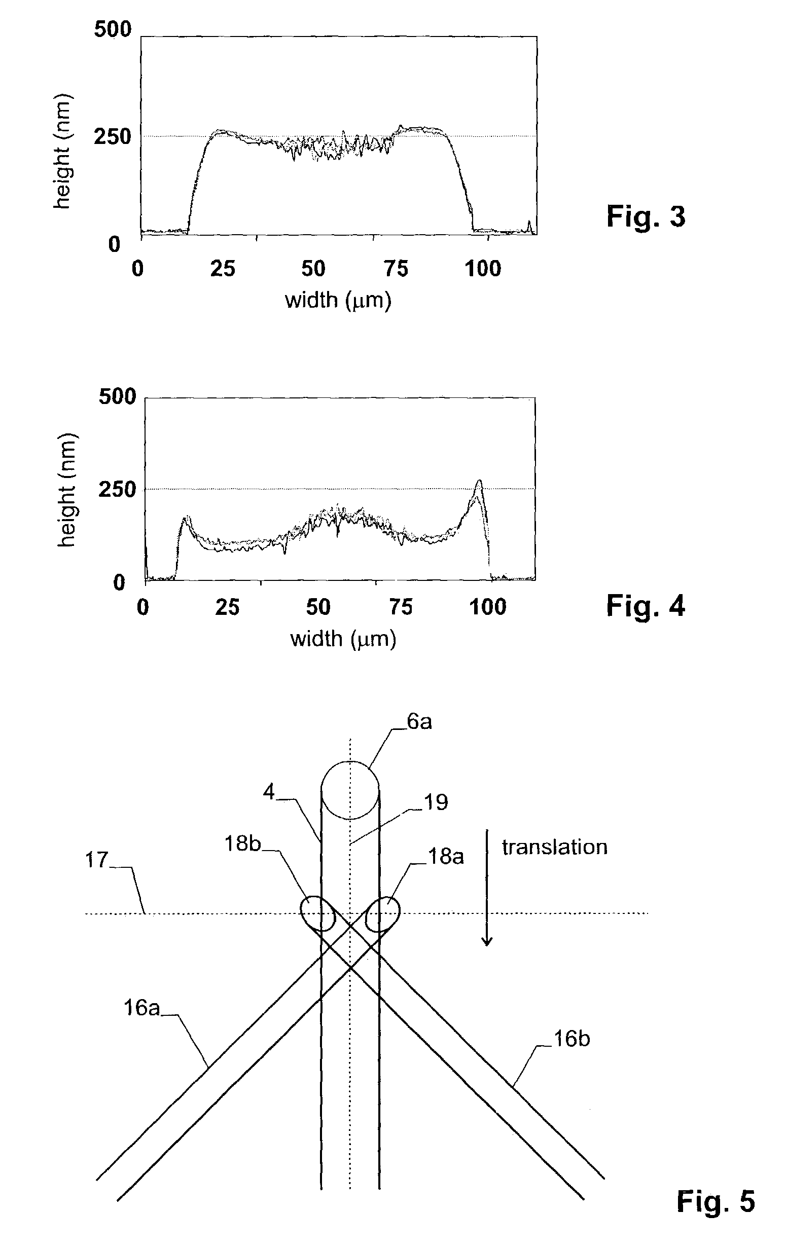
[0062]The same parameters as for example 2 were used, with the following exceptions: The translation speed was 0.2 mm / s and the laser power 300 mW. The thickness profile recorded by AFM is shown in FIG. 3.


PUM

PropertyMeasurementUnit
absorption coefficientaaaaaaaaaa
diameteraaaaaaaaaa
absorption coefficientaaaaaaaaaa

Abstract

For forming a fine structure of a desired material, nanoparticles of the same material are prepared in a suspension. A layer of the suspension is applied by a drop-on-demand printing system to a substrate. At least part of the layer is exposed to laser light for melting the nanoparticles at least partially. Upon solidification, the molten particles are sintered together to form the desired structure. Due to the low melting point of nanoparticles as compared to the melting point of bulk material, this procedure avoids damage to the substrate and provides a better control over the structure generation process. It can be used for generating metallic and non-metallic structures on various substrates. The laser light may have non-Gaussian intensity distribution or can combine multiple beams of Gaussian and non-Gaussian distribution for improving the quality of the generated structure, or it may be pulsed for improved control of the heat flow into the substrate.

Description

BACKGROUND OF THE INVENTION[0001]The present invention relates to a method for producing a structure by applying nanoparticles in a suspension onto a substrate and curing with laser radiation, and to the structures thereby produced.[0002]The term “nanoparticles” designates particles having a diameter well in the submicron range. It has been known that such particles exhibit thermophysical properties substantially different from those of the bulk materials. In particular, the melting point typically decreases substantially for particles having diameters below approximately 100 nm (nm=nanometer), and in particular below approximately 10 nm. For example, nanoparticles of gold show a melting point of approximately 300 to 400° C. at a diameter of approximately 2.5 nm while the bulk melting point of gold is 1063° C.[0003]In WO 00 / 10197 this effect is exploited for producing copper structures on a semiconductor wafer at low temperatures. A suspension of copper nanoparticles in a liquid is ...

Claims


Application Information

Patent Timeline
Patent Type & Authority Patents(United States)
IPC IPC(8): H01L21/44H01L21/48H01L21/768H05K3/10H05K3/12
CPCH01L21/4867H01L21/76838H05K3/125H05K3/105Y10S438/962B33Y10/00
Inventor GRIGOROPOULOS, CONSTANTINE P.BIERI, NICOLE RENEEPOULIKAKOS, DIMOSCHUNG, JAEWON
Owner RGT UNIV OF CALIFORNIA
Why Eureka
Try Eureka