Nanowire, circuit incorporating nanowire, and methods of selecting conductance of the nanowire and configuring the circuit

a technology of nanowires and conductances, applied in the direction of digital storage, instruments, semiconductor devices, etc., can solve the problems of difficult control of composition, memory can be difficult to scale to nanoscale dimensions, and additional circuitry

Inactive Publication Date: 2006-08-08
HEWLETT PACKARD DEV CO LP
View PDF0 Cites 82 Cited by
  • Summary
  • Abstract
  • Description
  • Claims
  • Application Information

AI Technical Summary

Benefits of technology

[0006]An exemplary embodiment of a nanowire comprises a single crystalline semiconductor material having an exterior surface and an interior region, and one or more dopant atoms. At least a portion of the nanowire thermally switches between two conductance states, the two conductance states being a high conductance state and a low conductance state. In the high conductance state, a first fraction of the dopant atoms are in the interior region and a second fraction of the dopant atoms are at the exterior surface. In the low conductance state, a third fraction of the dopant atoms are in the interior region and a fourth fraction of the dopant atoms are at the exterior surface. The first fraction is greater than the third fraction and the second fraction is less than the fourth fraction.
[0007]An exemplary embodiment of a circuit comprises a nanowire electrically connected between two electrical contact points within the circuit, the nanowire including a single crystalline semiconductor material having an exterior surface and an interior region, means for raising and lowering a temperature of at least a portion of the nanowire to switch at least the portion of the nanowire between two conductance states, the two conductance states being a high conductance state and a low conductance state, and a plurality of dopant atoms. In the high conductance state, a first fraction of the dopant atoms are in the interior region and a second fraction of the dopant atoms are at the exterior surface. In the low conductance state, a third fraction of the dopant atoms are in the interior region and a fourth fraction of the dopant atoms are at the exterior surface. The first fraction is greater than the third fraction and the second fraction is less than the fourth fraction.
[0008]An exemplary method to select the conductance of a nanowire formed of a single crystalline semiconductor material comprises increasing a temperature of the nanowire at least in a local region to a programming temperature to thermally activate diffusion of dopant atoms in the local region, and decreasing the temperature of the nanowire at least in the local region to a second temperature to immobilize dopant atoms in the local region, the second temperature being below the programming temperature. Increasing the temperature and decreasing the temperature thermally switches the nanowire between two conductance states, the two conductance states including a high conductance state and a low conductance state. In the high conductance state, a first fraction of the dopant atoms are in an interior portion of the local region and a second fraction of the dopant atoms are at an exterior surface of the local region. In the low conductance state, a third fraction of the dopant atoms are in the interior portion of the local region and a fourth fraction of the dopant atoms are at the exterior surface of the local region. The first fraction is greater than the third fraction and the second fraction is less than the fourth fraction.
[0009]An exemplary method to configure a circuit comprising a plurality of electrical paths formed of nanowires comprises selecting a first conductance of one or more nanowires in a first electrical path of the circuit, and changing the first conductance of the one or more nanowires in the first electrical path. The nanowires comprise a single crystalline semiconductor material having an exterior surface and an interior region, and one or more dopant atoms. The first conductance is one of a high conductance state and a low conductance state. In the high conductance state, a first fraction of the dopant atoms are in the interior region and a second fraction of the dopant atoms are at the exterior surface. In the low conductance state, a third fraction of the dopant atoms are in the interior region and a fourth fraction of the dopant atoms are at the exterior surface. The first fraction is greater than the third fraction and the second fraction is less than the fourth fraction.

Problems solved by technology

Generating the voltages on-chip from lower supply voltages can involve substantial additional circuitry; in addition these memories can be difficult to scale to nanoscale dimensions.
Phase-change materials can involve complex combinations of elements, some of which may be toxic, and control of the composition can be difficult.

Method used


Image

  • Nanowire, circuit incorporating nanowire, and methods of selecting conductance of the nanowire and configuring the circuit
  • Nanowire, circuit incorporating nanowire, and methods of selecting conductance of the nanowire and configuring the circuit
  • Nanowire, circuit incorporating nanowire, and methods of selecting conductance of the nanowire and configuring the circuit

Examples


Embodiment Construction

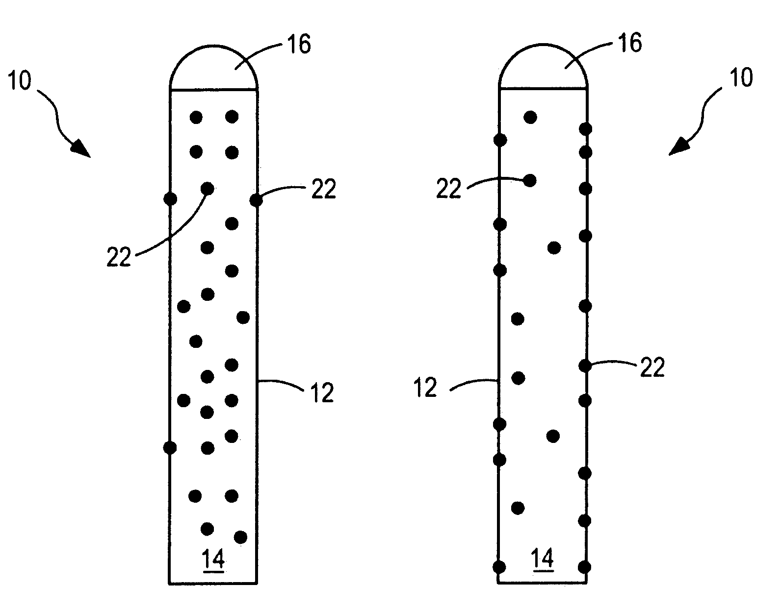
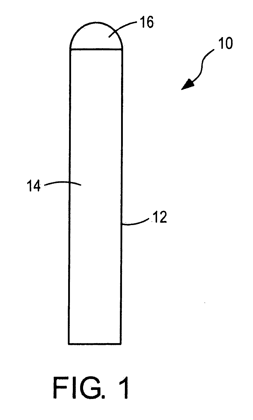
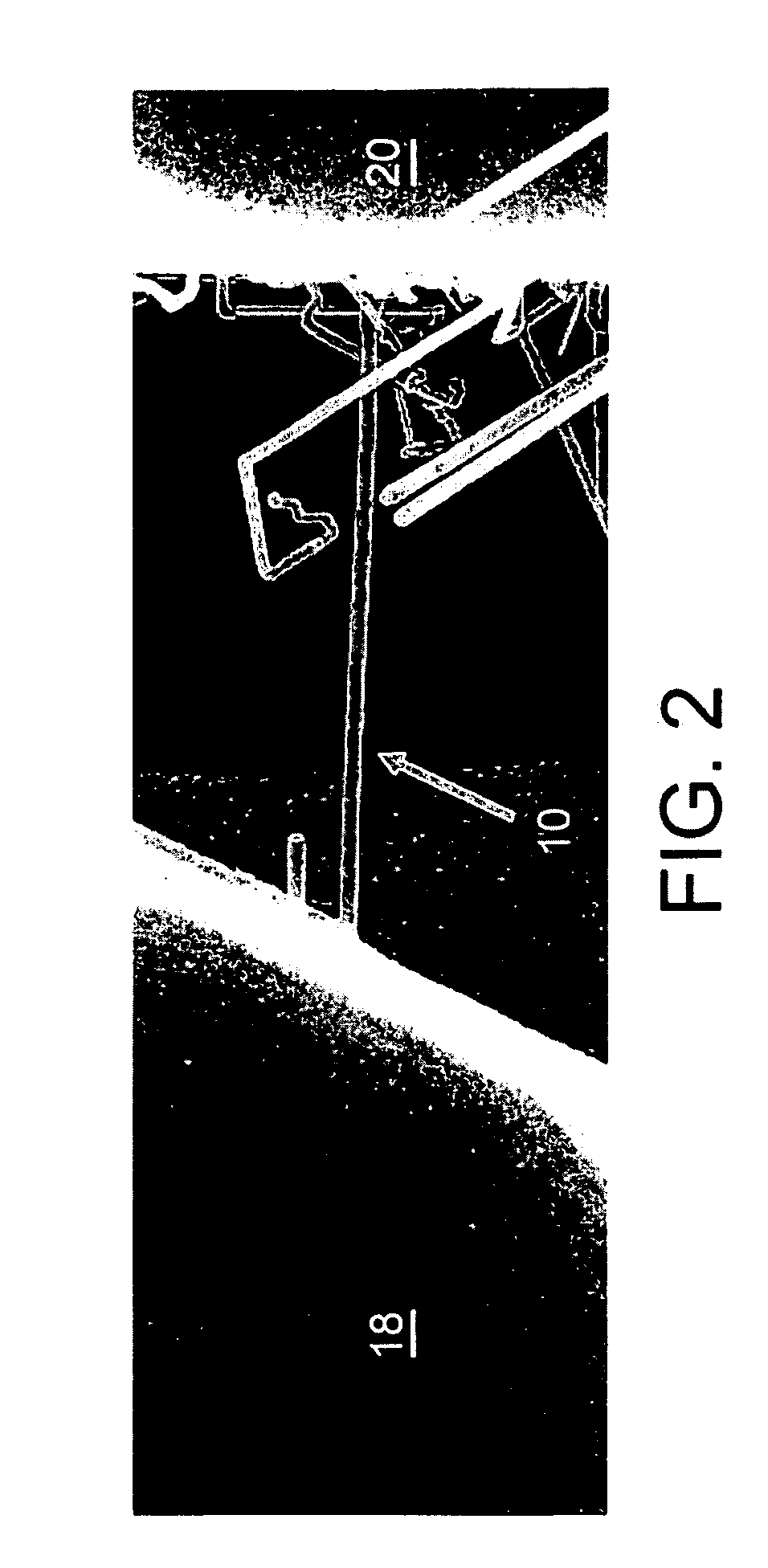
[0022]An exemplary embodiment of a nanowire is schematically illustrated in FIG. 1. The exemplary embodiment of a nanowire 10 comprises a single crystalline semiconductor material having an exterior surface 12 and an interior region 14. In one embodiment, the nanowire 10 is columnar in shape and has a catalyst nanoparticle 16 at one end as a result of the metal catalyzed deposition process. FIG. 2 is a micrograph showing a nanowire 10 connecting between two electrodes 18, 20.

[0023]The nanowire contains dopant atoms. When in the interior region of the semiconductor material, the dopant atoms increase the conductance of the material. Conversely, when at the exterior surface of the semiconductor material, the dopant atoms do not increase the conductance of the material. In exemplary embodiments, the nanowires have a variable conductance state dependent on the number or concentration of dopant atoms at different regions of the nanowire. For example, the exemplary embodiments of nanowire...


PUM

PropertyMeasurementUnit
diameteraaaaaaaaaa
diameteraaaaaaaaaa
programming temperatureaaaaaaaaaa

Abstract

A nanowire includes a single crystalline semiconductor material having an exterior surface and an interior region and at least one dopant atom. At least a portion of the nanowire thermally switches between two conductance states; a high conductance state, where a high fraction of the dopant atoms is in the interior region, and a low conductance state, where a lower fraction of the dopant atoms is at the interior region and a higher fraction of the atoms is at the exterior surface. A method to select the conductance of the nanowire increases a temperature of the nanowire at least in a local region to a programming temperature to thermally activate diffusion of a dopant atom into a bulk region of the single crystalline semiconductor material and decreases the temperature of the nanowire at least in the local region to a second temperature to immobilize dopant atoms in the bulk region, the second temperature being below the programming temperature, wherein immobilized dopant atoms in the bulk region produce a desired high or low conductance state in the nanowire. The method can be used to initially configure and to reconfigure a circuit incorporating the nanowire.

Description

BACKGROUND[0001]1. Field[0002]The present disclosure relates to nanostructures and programmable electronic devices incorporating nanostructures, e.g., nanoelectronic devices incorporated into a circuit.[0003]2. Background Information[0004]“Top-down” approaches to increasing electronic device density are known. An alternative “bottom-up” technological approach uses functional nano-structures assembled from chemically synthesized, nano-scale building blocks. Wide-scale integration of functional nano-scale devices involves connecting nanoscale electrically conducting wires to microscale electrodes. One approach to address this connectivity issue is the simultaneous lateral growth of a high density of highly oriented, metal catalyzed silicon nanowires on a patterned substrate where the nanowires are between two vertical sidewalls.[0005]Known attempts to program the conductivity of a device element have used charge storage in an isolated region to control the conduction in a nearby semic...

Claims


Application Information

Patent Timeline
Patent Type & Authority Patents(United States)
IPC IPC(8): H01L29/02
CPCB82Y10/00H01L45/165G11C13/025H01L29/0665H01L29/0673H01L29/0676H01L29/685H01L45/08H01L45/085H01L45/1226H01L45/1233H01L45/148H01L45/1616G11C13/02G11C2213/16G11C2213/17H01L29/78696Y10S977/762Y10S977/943Y10S977/938H10N70/24H10N70/245H10N70/823H10N70/826H10N70/884H10N70/023H10N70/043
Inventor KAMINS, THEODORE I.
Owner HEWLETT PACKARD DEV CO LP
Why Eureka
Try Eureka