

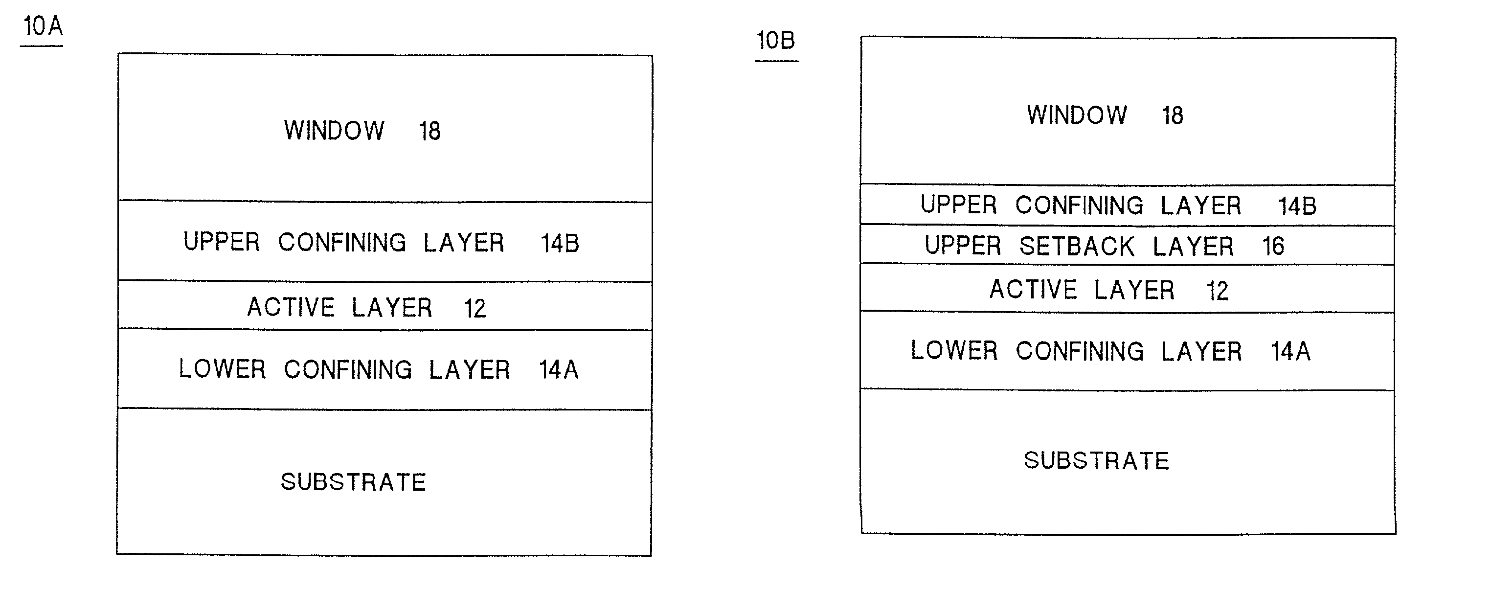
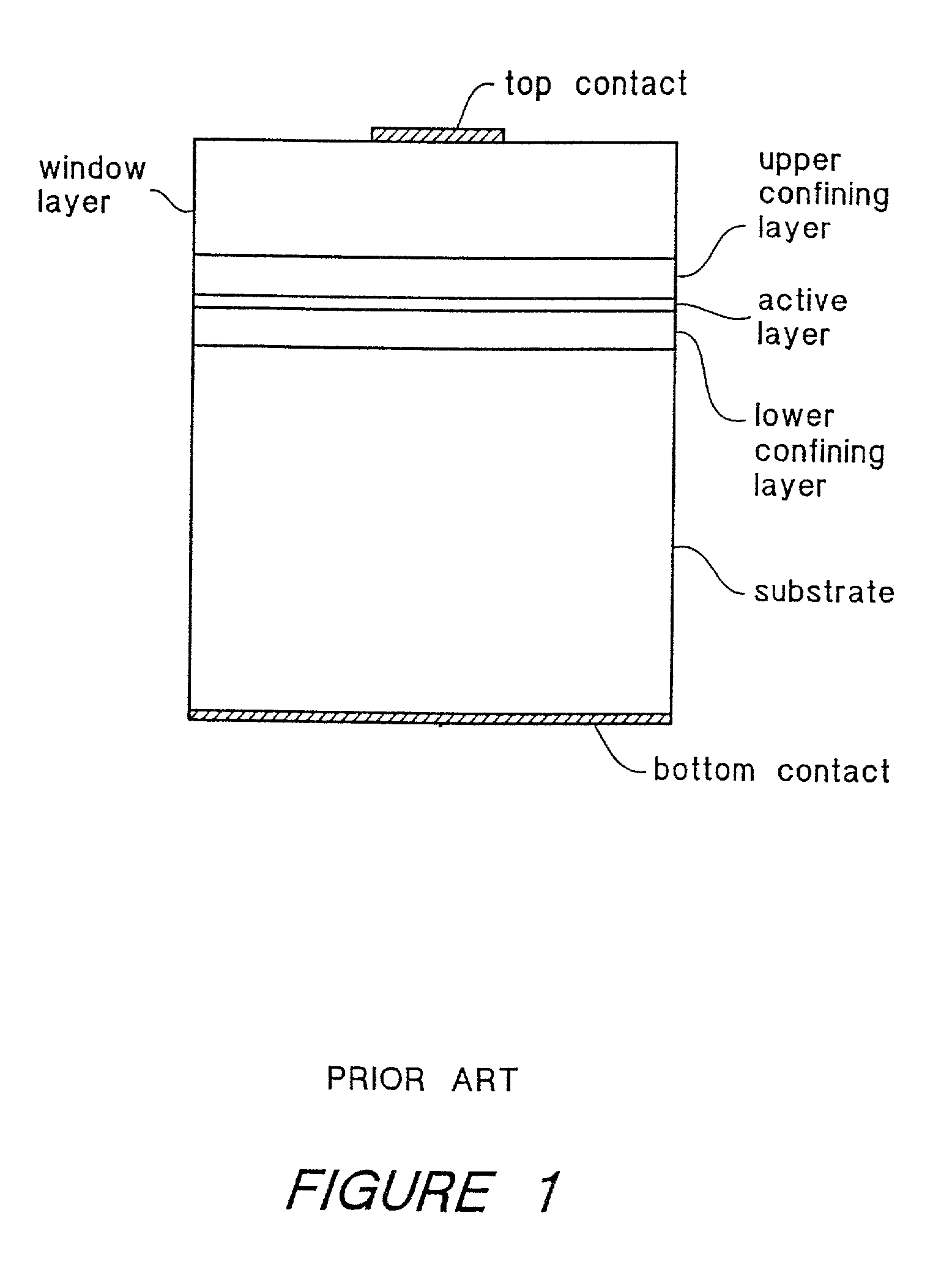
Lll-phosphide light emitting devices with thin active layers
a technology of phosphide and active layer, which is applied in the direction of semiconductor/solid-state device manufacturing, semiconductor devices, electrical devices, etc., can solve the problems of reducing the sensitivity of the internal quantum efficiency to changes, and reducing the internal quantum efficiency of the led. , to achieve the effect of increasing the extraction efficiency, reducing the internal quantum efficiency of the led, and improving the extraction efficiency
- Summary
- Abstract
- Description
- Claims
- Application Information
AI Technical Summary
Benefits of technology
Problems solved by technology
Method used
Image

Examples
Embodiment Construction
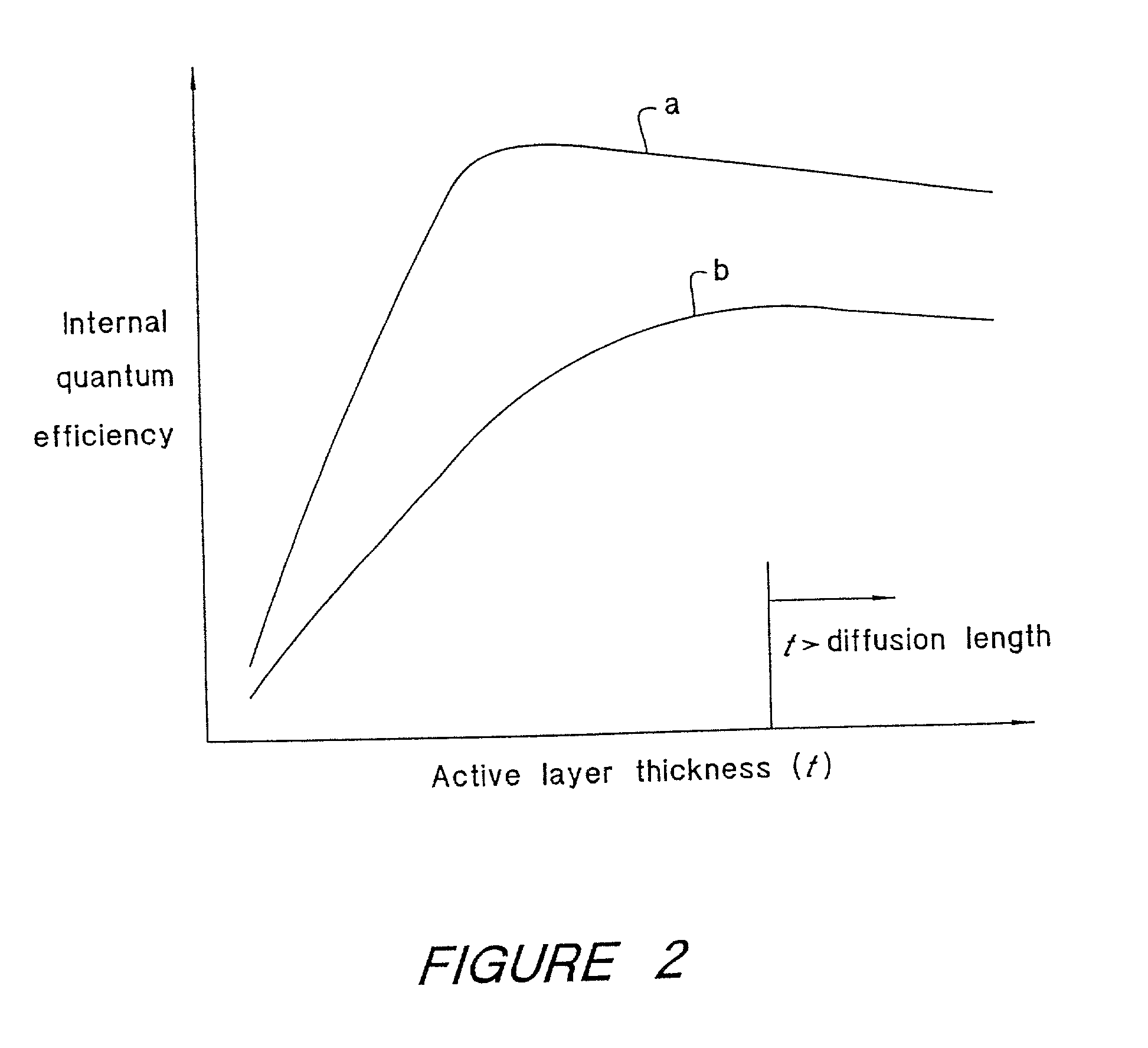
[0030]FIG. 4 shows the dependence of internal quantum efficiency, extraction efficiency, and external quantum efficiency on the thickness of the active layer for an AlGaInP transparent substrate light emitting diode (TS-LED). The external quantum efficiency is the product of the internal quantum efficiency and the extraction efficiency:
ηexternal=ηinternal×ηextraction
For one range of active layer thicknesses shown in FIG. 4, the external quantum efficiency is limited by the internal quantum efficiency, and in another range of thicker active layers, the external quantum efficiency is limited by the extraction efficiency. A TS-LED with optimal external quantum efficiency has an active layer thickness that is chosen to balance the influence of internal quantum efficiency and extraction efficiency, as shown by Point A. In contrast, an AS-LED with optimal external quantum efficiency also has optimal internal quantum efficiency and the active layer thickness is chosen to maximize this effi...
PUM
 Abstract
Description
Claims
Application Information