

Termination structure of DMOS device
a technology of dmos and structure, applied in the direction of semiconductor/solid-state device manufacturing, semiconductor devices, electrical equipment, etc., can solve the problems of easy electric breakdown, more lithographic processes in the process of forming trenched power transistors, and difficult device design, etc., to achieve uniform dopant concentration
- Summary
- Abstract
- Description
- Claims
- Application Information
AI Technical Summary
Benefits of technology
Problems solved by technology
Method used
Image

Examples
Embodiment Construction
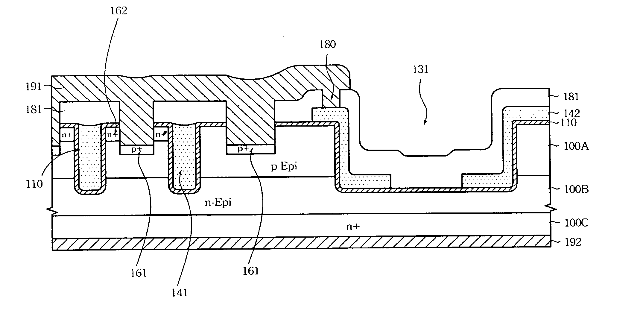
[0025]The exemplary embodiment of the invention disclosed herein is directed to a termination structure of DMOS device. In the following description, numerous details are set forth in order to provide a clear understanding of the present invention. It will be appreciated by one skilled in the art that variations of these specific details are possible while still achieving the results of the present invention. In other instance, well-known components are not described in detail in order not to unnecessarily obscure the present invention.
[0026]As illustrated in FIGS. 4A through 4F, a sequence for forming a trenched DMOS and a termination structure is disclosed in accordance with the exemplary embodiment of the present invention.
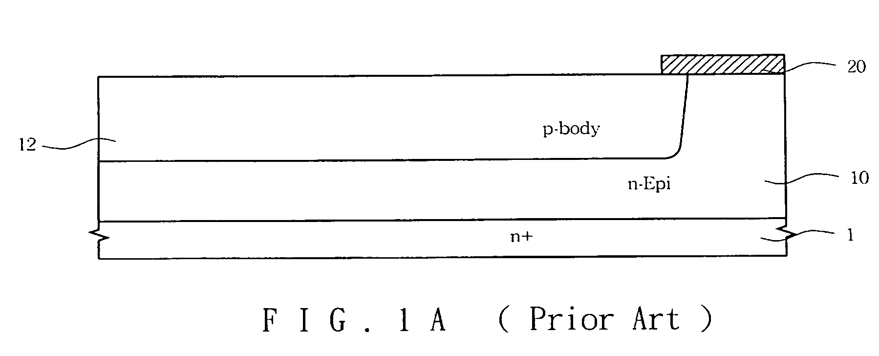
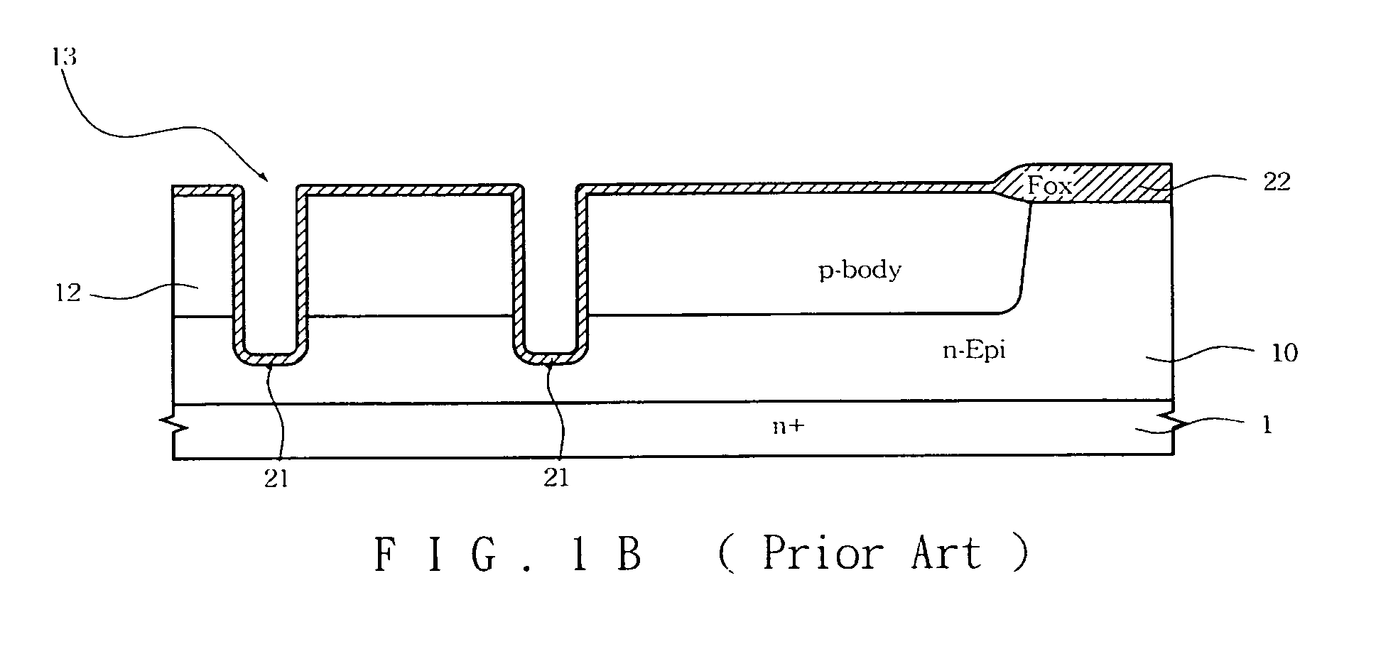
[0027]In FIG. 4A, a first epitaxial layer 100B with N-type doping and a second epitaxial layer 100A with P-type doping are sequentially formed on the surface of an N+ silicon substrate 100C. The first epitaxial layer 100B and the second epitaxial layer 100A are...
PUM
 Abstract
Description
Claims
Application Information