Integrated circuit package and method of manufacture

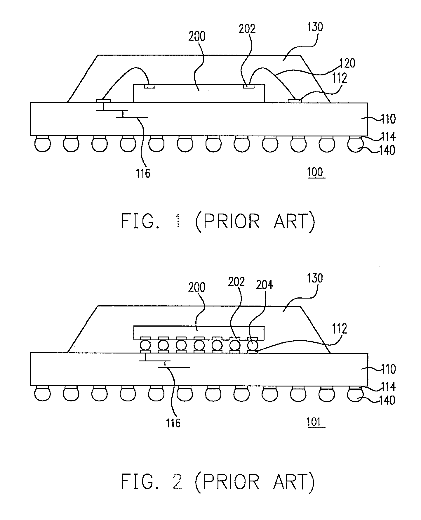
a technology of integrated circuits and manufacturing methods, applied in the direction of printed circuit manufacturing, electrical apparatus construction details, printed circuit non-printed electric components association, etc., can solve the problems of increasing the number of manufacturing steps, affecting the performance of the chip, and the package that uses conductive wires to connect with the chip has a bigger signaling time delay, so as to reduce the production cost of the integrated circuit package and eliminate the requirement of connective elements , the effect of increasing the performance of the packag

Inactive Publication Date: 2006-08-08
VIA TECH INC
View PDF10 Cites 80 Cited by
  • Summary
  • Abstract
  • Description
  • Claims
  • Application Information

AI Technical Summary

Benefits of technology

[0011]Accordingly, one object of the present invention is to provide an integrated circuit package and its method of manufacture. The package eliminates the connective requirements between a substrate and a silicon chip such as wire bonding or flip-chip bonding but still manages to tolerate the contact point pitch originally used by the substrate. Hence, production cost of the integrated circuit package is reduced and performance of the package is increased. Furthermore, the IC package has a higher heat dissipation rate and engenders less limitation due to flip-chip bumps.

Problems solved by technology

In general, a ball grid array package that uses conductive wires to connect with the chip has bigger signaling time delay due to higher electrical impedance of conductive wires.
Hence, performance of the chip may be affected.
Therefore, the number of manufacturing steps is increased and production cost is ultimately raised.
Therefore, compared with a conventional printed circuit board, cost of producing the substrate with fine pitch contacts is considerably higher.
The fabrication cost is estimated to be about 20% of the cost of forming the entire ball grid array package.
The cost of fabricating a substrate suitable for forming a flip-chip package is even higher.

Method used


Image

  • Integrated circuit package and method of manufacture
  • Integrated circuit package and method of manufacture
  • Integrated circuit package and method of manufacture

Examples


Embodiment Construction

[0022]Reference will now be made in detail to the present preferred embodiments of the invention, examples of which are illustrated in the accompanying drawings. Wherever possible, the same reference numbers are used in the drawings and the description to refer to the same or like parts.

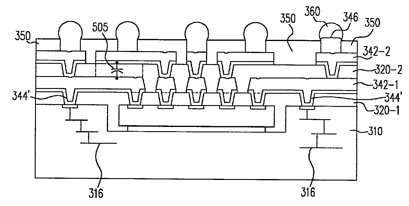
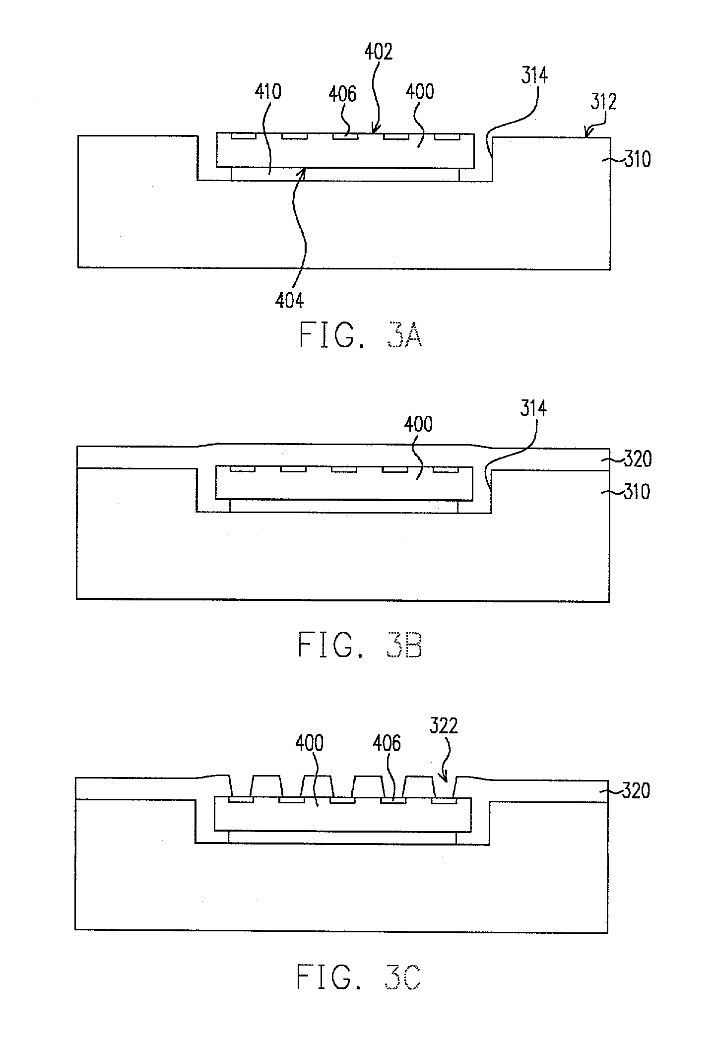
[0023]FIGS. 3A to 3I are schematic cross-sectional views showing the progression of steps for producing an integrated circuit package according to one preferred embodiment of this invention. As shown in FIG. 3A, a substrate 310 having a cavity 314 thereon is selectively provided. The cavity 314 is on the upper surface 312 of the substrate 310 but does not have to be located right in the middle of the substrate 310 as shown in FIG. 3A. In addition, a chip 400 having an active surface 402 and a backside surface 404 is also provided. The backside 404 of the chip 400 is attached to the bottom surface of the cavity 314. However, the chip may also be attached to the upper surface 312 of the substrate 310 s...


PUM

PropertyMeasurementUnit
widthaaaaaaaaaa
widthaaaaaaaaaa
widthaaaaaaaaaa

Abstract

An integrated circuit package and a method of manufacturing the package. A silicon chip is attached to the surface of a substrate or attached to the bottom surface of a cavity in the substrate so that the active surface of the chip is exposed. One or more build-up circuit structures are formed over the substrate. Each build-up circuit structure has at least one insulation layer, at least one patterned circuit layer and a plurality of via openings with conductive material therein so that bonding pads on the active surface of the chip connect electrically with the patterned circuit layer through the vias. To form a ball grid array package, solder balls may also be attached to the solder ball pads on the patterned circuit layer so that the bonding pads on the chip are electrically connected to an external circuit through the build-up circuit structure and the solder balls.

Description

CROSS REFERENCE TO RELATED APPLICATIONS[0001]This application claims the priority benefit of Taiwan application Serial no. 91100554, filed Jan. 16, 2002.BACKGROUND OF INVENTION[0002]1. Field of Invention[0003]The present invention relates to an integrated circuit package and method of manufacture. More particularly, the present invention relates to an integrated circuit package having a built-up circuit instead of a conventional substrate and a method of manufacturing the integrated circuit package.[0004]2. Description of Related Art[0005]In step with the rapid progress in electronic technologies, high-tech electronic products having more powerful and personalized functions continue to appear in the market. In general, electronic products are designed towards having a lower dead weight, a smaller and slimmer outline, and being easier to carry. The manufacturing of integrated circuits (IC) is a major stage in fabricating most electronic products. ICs may be packaged into a variety of...

Claims


Application Information

Patent Timeline
Patent Type & Authority Patents(United States)
IPC IPC(8): H01L23/522H01L21/60H01L23/498H01L23/538
CPCH01L24/19H01L24/24H01L23/5389H01L23/49816Y10T29/4913H01L2224/04105H01L2224/16227H01L2224/20H01L2224/24227H01L2224/48091H01L2224/48227H01L2224/73267H01L2224/92244H01L2924/01029H01L2924/01075H01L2924/01082H01L2924/14H01L2924/15153H01L2924/15165H01L2924/1517H01L2924/15311H01L2924/19041H01L2924/19042H01L2924/30105H01L2924/3011H01L2924/3025Y10T29/49165H01L2224/0401H01L2224/24226H01L2924/10253H01L2224/32225H01L2224/16225H01L2924/01047H01L2924/01033H01L2924/00015H01L2924/00H01L2924/12042H01L2924/181
Inventor CHEN, KUO-TSOKUNG, CHEN-YUEH
Owner VIA TECH INC
Why Eureka
Try Eureka