High-gain, bulk-driven operational amplifiers for system-on-chip applications

a technology of operational amplifiers and system-on-chips, applied in the direction of dc-amplifiers with dc-coupled stages, amplifiers with semiconductor devices/discharge tubes, different amplifiers, etc., can solve the problems of low gain disadvantage of bulk-driven techniques and inherently poor so as to reduce the threshold limitation of mosfet transistors and improve the gain of bulk-driven amplifiers. , the effect of increasing th

Inactive Publication Date: 2006-08-08
UNIVERSITY OF ROCHESTER
View PDF2 Cites 23 Cited by
  • Summary
  • Abstract
  • Description
  • Claims
  • Application Information

AI Technical Summary

Benefits of technology

[0009]It is thus an object of the present invention to improve the gain of bulk-driven amplifiers. To achieve the above and other objects, the present invention is directed to an ultra-low voltage rail-to-rail operational transconductance amplifier (OTA) which can be based on a standard digital 0.18 μm CMOS process. To achieve rail-to-rail opera-tion, complementary input differential pairs are used, where the bulk-driven technique is applied to reduce the threshold limitation of the MOSFET transistors. The OTA gain is increased by using auxiliary gain boosting amplifiers. This additional circuitry enables the OTA to operate at 0.8 volts, achieving an open loop gain of 68 dB while consuming 94 μW. The DC gain of the amplifier is the highest gain achieved to date in bulk-driven amplifiers.
[0011]The design of an ultra-low voltage, high performance folded-cascode OTA circuit in a standard digital CMOS process will be disclosed. To accommodate a low power supply voltage (0.8 volt), the bulk-driven MOSFET approach is used. The low gain disadvantage of the bulk-driven technique is circumvented by employing gain boosting amplifiers, permitting the achievement of a DC gain of 68 dB. Due to a lower body transconductance, bulk-driven amplifiers inherently exhibit relatively poor gain. The low gain is the primary reason why amplifiers reported in Blalock et al and in Bahmani et al have only exhibited a DC gain as high as 45 dB. The present invention offers an advantage in that that bulk-driven amplifiers can be modified to operate with low power supply voltages while still exhibiting performance levels that satisfy the demands of state-of-the-art mixed-signal circuits.

Problems solved by technology

The low gain disadvantage of the bulk-driven technique is circumvented by employing gain boosting amplifiers, permitting the achievement of a DC gain of 68 dB.
Due to a lower body transconductance, bulk-driven amplifiers inherently exhibit relatively poor gain.

Method used


Image

  • High-gain, bulk-driven operational amplifiers for system-on-chip applications
  • High-gain, bulk-driven operational amplifiers for system-on-chip applications
  • High-gain, bulk-driven operational amplifiers for system-on-chip applications

Examples


Embodiment Construction

[0019]A preferred embodiment of the present invention will be set forth in detail with reference to the drawings, in which like reference numerals refer to like elements throughout.

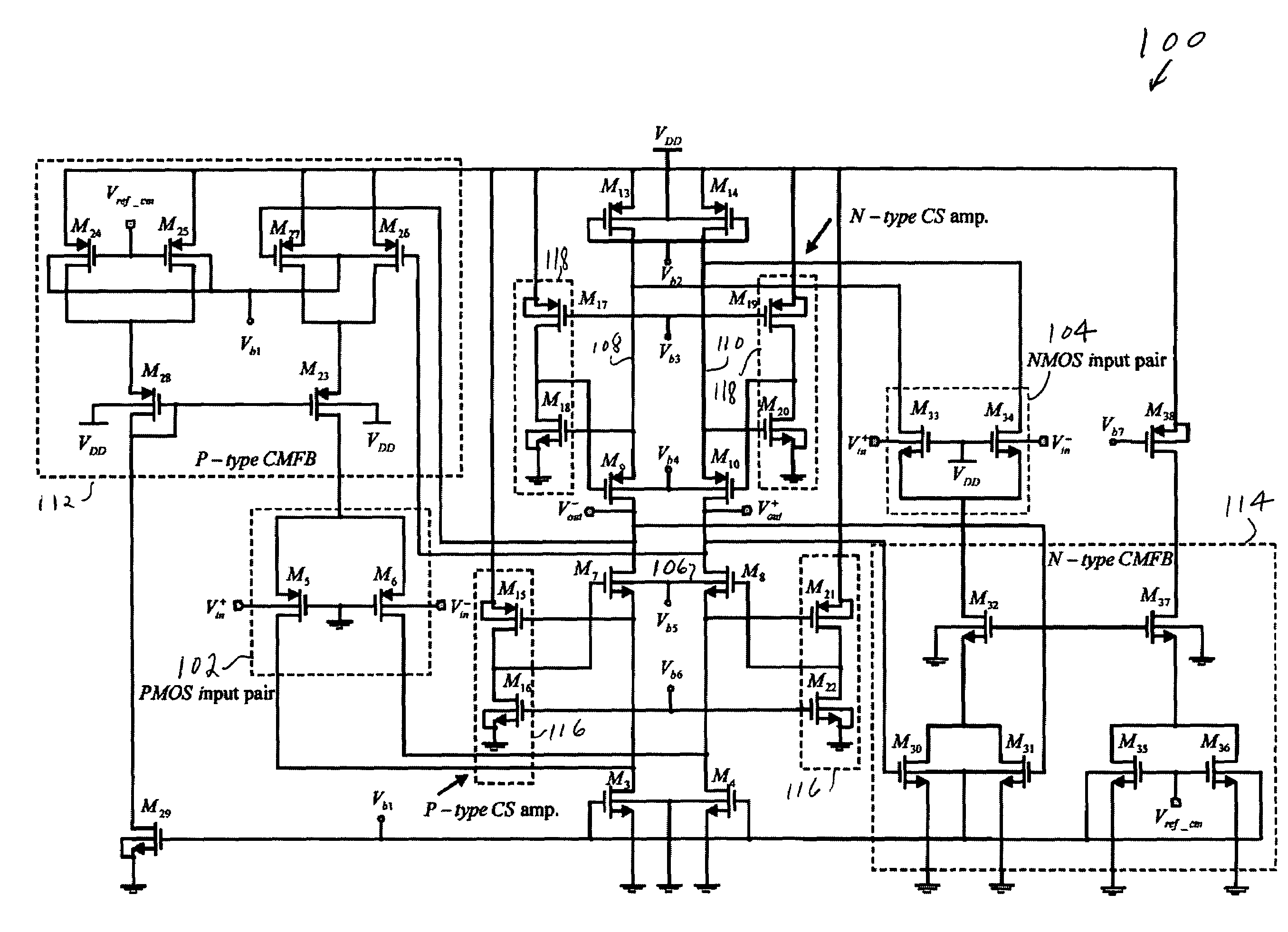
[0020]The amplifier core 100 of an OTA is illustrated in FIG. 1. This circuit is based on a fully differential topology with two complementary input pairs 102, 104. The output branch 106 includes common gate amplifiers M7, M8 with cascode current loads 108, 110 to increase the gain. A common mode feedback circuit (CMFB) 112, 114 is used with four auxiliary common source amplifiers. The operation of the OTA is explained in greater detail below.

[0021]Rail-to-rail operation is achieved using a pair of PMOS (102; M5 and M6) and NMOS (104; M33 and M34) transistors at the input stage. This strategy supports rail-to-rail (0 volt to 0.8 volt) operation of the amplifier; thus, the input common mode range (ICMR) is extended to the largest possible range. This increased range is achieved because when the input commo...


PUM


Abstract

An ultra-low voltage rail-to-rail operational transconductance amplifier (OTA) is based on a standard digital 0.18 μm CMOS process. Techniques for designing a 0.8 volt fully differential OTA include bias and reference current generator circuits. To achieve rail-to-rail operation, complementary input differential pairs are used, where the bulk-driven technique is applied to reduce the threshold limitation of the MOSFET transistors. The OTA gain is increased by using auxiliary gain boosting amplifiers.

Description

REFERENCE TO RELATED APPLICATION[0001]The present application claims the benefit of U.S. Provisional Patent Application No. 60 / 479,506, filed Jun. 19, 2003, whose disclosure is hereby incorporated by reference in its entirety into the present disclosure.STATEMENT OF GOVERNMENT INTEREST[0002]The work leading to the present invention was supported in party by the DARPA / ITO under AFRL Contract F29601-00-K-0182, the National Science Foundation under Contract No. CCR-0304574, and the Fulbright Program under Grant No. 87481764. The government has certain rights in the invention.FIELD OF THE INVENTION[0003]The present invention is directed to a bulk-driven operational amplifier and more particularly to such an amplifier exhibiting high gain, suitable for use in system-on-chip applications requiring low power.DESCRIPTION OF RELATED ART[0004]The reduction in the minimum dimensions in VLSI technologies, along with the trend of using small portable devices, necessitates reduced power supply vo...

Claims


Application Information

Patent Timeline
IPC IPC(8): H03F3/45
CPCH03F3/45659H03F3/45219
Inventor ROSENFELD, JONATHANKOZAK, MUCAHITFRIEDMAN, EBY G.
Owner UNIVERSITY OF ROCHESTER
Why Eureka
Try Eureka