

Ultra thin body fully-depleted SOI MOSFETs
a soi mosfet, fully depleted technology, applied in the direction of basic electric elements, semiconductor devices, electrical equipment, etc., can solve the problems that the prior art method cannot be extended any further, and the threshold voltage variation of fully depleted soi mosfet devices with doped channels is typically very large, so as to reduce the threshold voltage variation, improve the control in the recessed channel step, and reduce the effect of threshold voltage variation
- Summary
- Abstract
- Description
- Claims
- Application Information
AI Technical Summary
Benefits of technology
Problems solved by technology
Method used
Image

Examples
Embodiment Construction
[0030]The present invention, which provides a method for threshold voltage variations control in ultra thin fully-depleted SOI MOSFETs, will now be described in greater detail by referring to the drawings that accompany the present application.
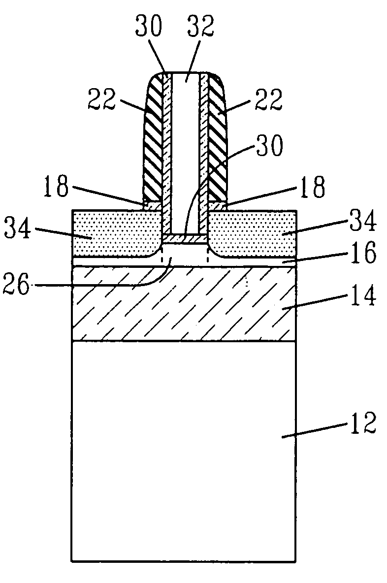
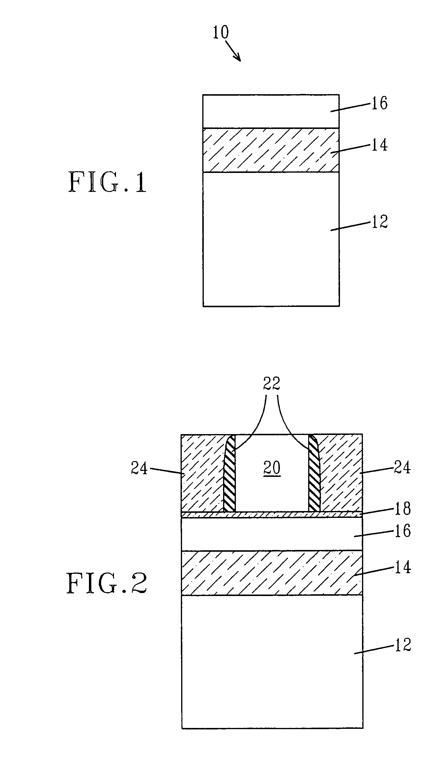
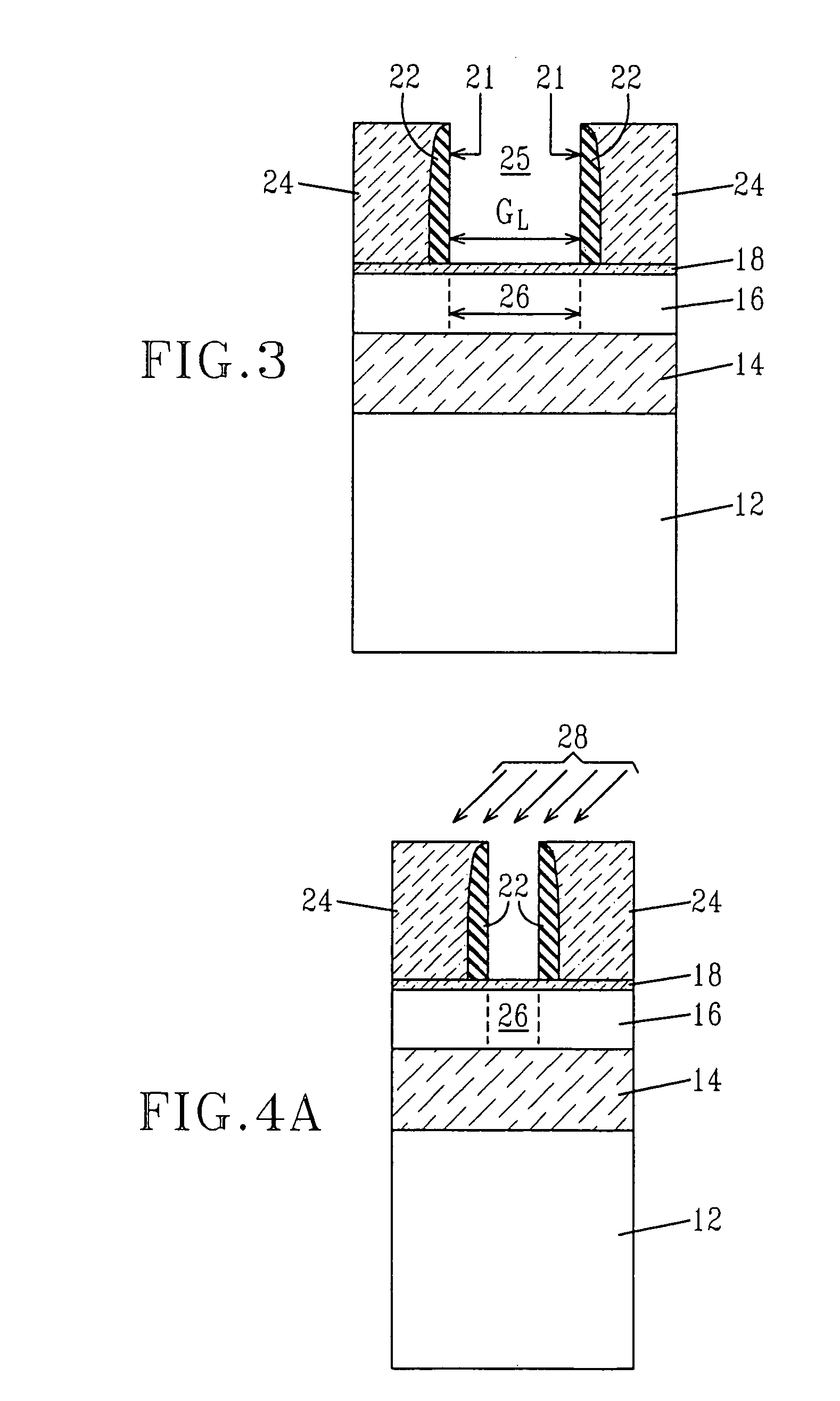
[0031]Referring to FIG. 1 there is shown an initial SOI substrate 10 that can be employed in the present invention. The initial SOI substrate 10 includes a bottom Si-containing layer 12, a buried insulating layer 14, such as an oxide or nitride, located on the bottom Si-containing layer 12, and a top Si-containing layer 16, i.e., the SOI layer, located on the buried insulating layer 14. The term “Si-containing layer” denotes any material that includes silicon. Illustrative examples of Si-containing materials include, but are not limited to: Si, SiGe, SiGeC, SiC, polysilicon, i.e., polySi, epitaxial silicon, i.e., epi Si, amorphous silicon, i.e., a:Si, and multilayers thereof. Typically, layers 12 and 16 of the SOI substrate 10 are both compris...
PUM
 Abstract
Description
Claims
Application Information