Heat treatment apparatus by means of light irradiation

Active Publication Date: 2006-08-15
SCREEN HLDG CO LTD
View PDF16 Cites 17 Cited by
  • Summary
  • Abstract
  • Description
  • Claims
  • Application Information

AI Technical Summary

Benefits of technology

[0017]When the substrate cracks to litter the chamber with its fragments, the chamber can be easily cleaned by simply detaching the liner from the chamber.
[0018]It is therefore an object of the present invention to provide a heat treatment appar

Problems solved by technology

Temperature rise in a very short period of time by use of a xenon flash lamp does not allow a period long enough for ion diffusion, thereby realizing ion activation with no rounding of a profile of ions implanted into a semiconductor wafer.
The light emitted from the xenon flash lamp has considerably high intensity, which may result in generation of a brown oxide film during heat treatment that covers a metal surface inside the chamber.
Even a slight source of contamination may result in imperfect treatment in light of recent trends toward high precision of a semiconductor device, for example.
Generation of such an oxide film is thus unfavorable.
In addition to the foregoing adherence of a deposited material, contamination of a heat treatment chamber results from various reason

Method used


Image

  • Heat treatment apparatus by means of light irradiation
  • Heat treatment apparatus by means of light irradiation
  • Heat treatment apparatus by means of light irradiation

Examples


Example

[0025]The preferred embodiment of the present invention will be described in detail with reference to the drawings.

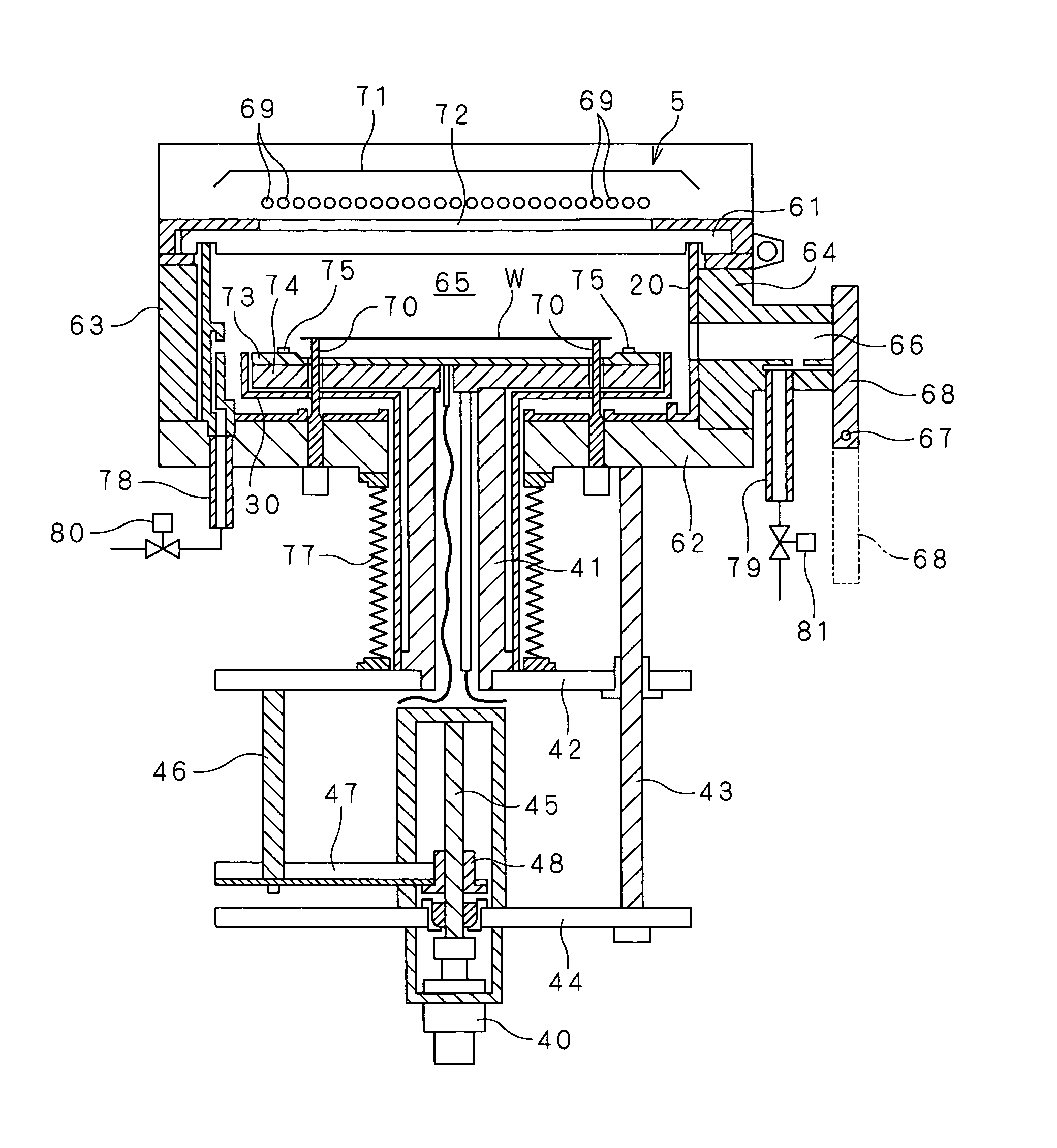
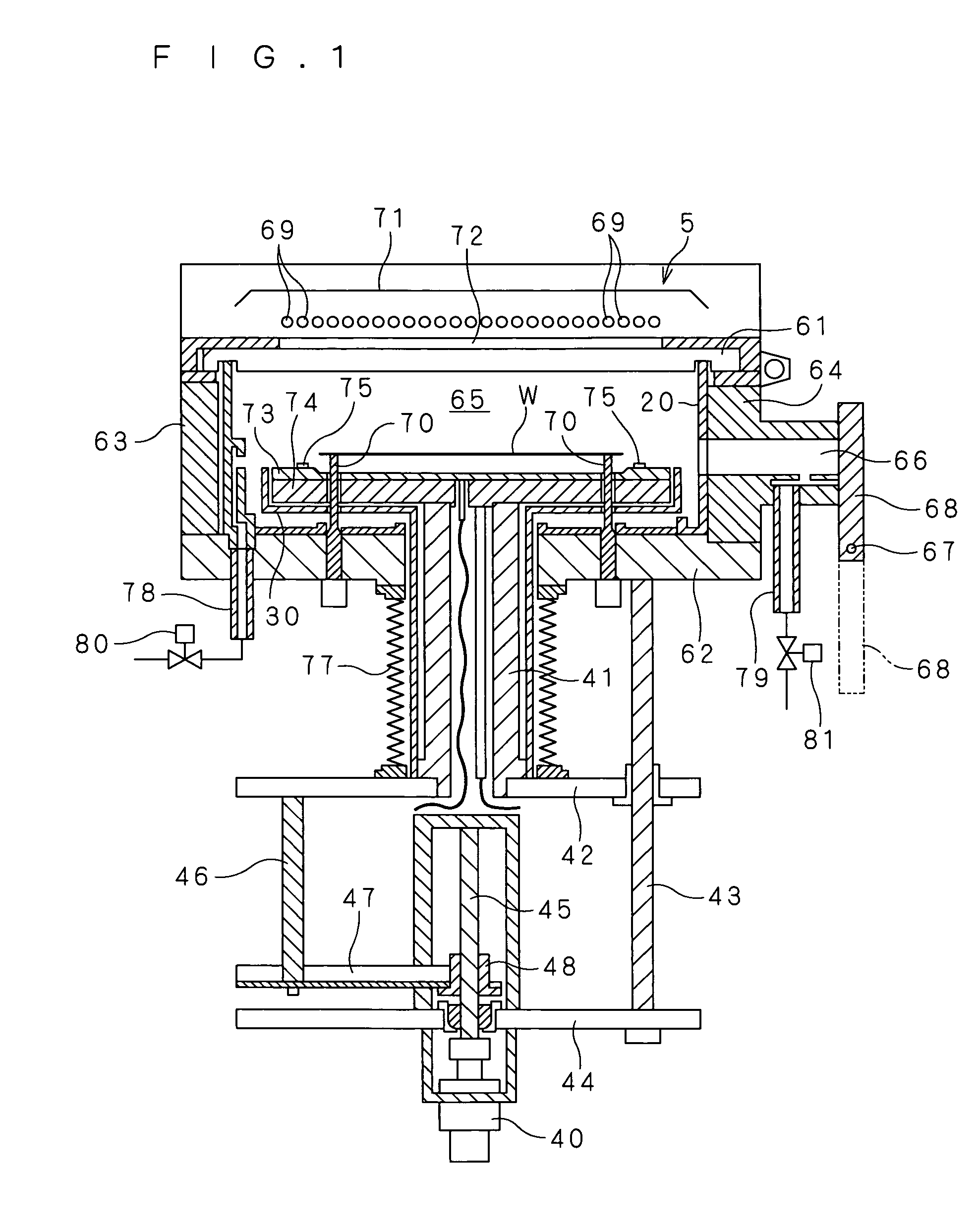
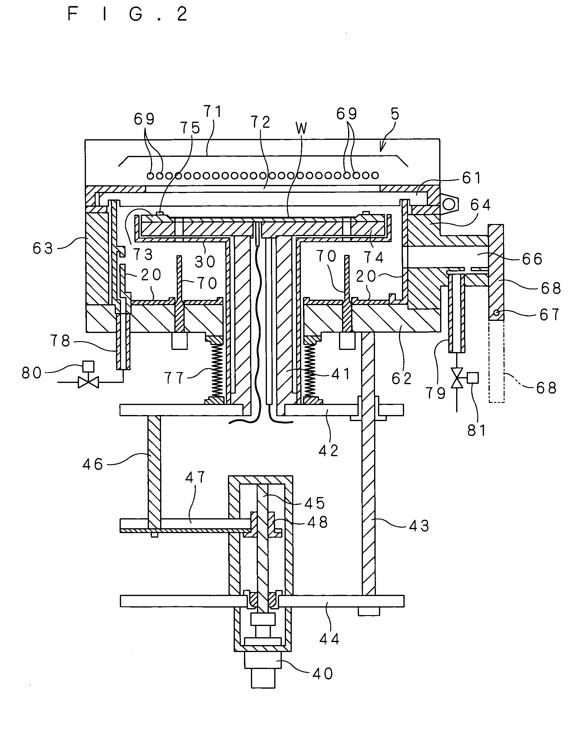
[0026]FIGS. 1 and 2 are side sectional views each showing the configuration of a heat treatment apparatus according to the present invention which is intended for heat treatment of a substrate such as a semiconductor wafer by means of irradiation with flashlight emitted from a xenon flash lamp.

[0027]The heat treatment apparatus of the present invention comprises a chamber 65 for heat treatment of a semiconductor wafer W stored therein. The chamber 65 is formed by a translucent plate 61, a base plate 62, and a pair of side plates 63 and 64. As an example, the translucent plate 61 as the upper portion of the chamber 65 includes an infrared-transparent material such as quartz. The translucent plate 61 is operative to function as a chamber window for allowing light emitted from a light source 5 to pass therethrough to be guided to the chamber 65. As an example, the base pla...


PUM

PropertyMeasurementUnit
Surface roughnessaaaaaaaaaa
Shapeaaaaaaaaaa
Surface smoothnessaaaaaaaaaa

Abstract

A chamber has a wall surface fitted with a liner. The liner is removably provided to the chamber with no fixed relation therebetween. By simply opening a light source to remove a heat diffusion plate, a hot plate and a tubular member from the chamber, the liner can be easily detached accordingly from the chamber. When a semiconductor wafer cracks to litter the chamber with its fragments, the chamber can be easily cleaned by simply detaching the liner. The liner has an outer surface subjected to surface roughening by honing. When a flash lamp emits flashlight of considerably high intensity, the roughened outer surface of the liner serves to block this flashlight. As a result, the metal surface inside the chamber is prevented from being exposed to the flashlight emitted from the flash lamp.

Description

BACKGROUND OF THE INVENTION[0001]1. Field of the Invention[0002]The present invention relates to a heat treatment apparatus for heat-treating a semiconductor wafer or a glass substrate (hereinafter simply referred to as a “substrate”) by means of light irradiation thereon.[0003]2. Description of the Background Art[0004]Conventional ion activation process of a semiconductor wafer after being subjected to ion implantation employs a heat treatment apparatus such as a lamp annealing apparatus using a halogen lamp. In such a heat treatment apparatus, a semiconductor wafer is heated up (annealed) to a temperature of about 1000 to 1100° C. to realize ion activation of the semiconductor wafer. Light energy emitted from the halogen lamp is operative to cause temperature rise of the wafer at a speed of about several hundreds of degrees centigrade per second.[0005]An example of a lamp annealing apparatus using a halogen lamp is introduced in Japanese Patent Application Laid-Open No. 2001-12700...

Claims


Application Information

Patent Timeline
IPC IPC(8): F27B5/14F27B17/00H01L21/324F27D11/00H01L21/00
CPCH01L21/67115F27B17/0025H01L21/324
Inventor MURAYAMA, HIROMIKUSUDA, TATSUFUMI
Owner SCREEN HLDG CO LTD
Why Eureka
Try Eureka