Variable voltage supply bias and methods for negative differential resistance (NDR) based memory device

a memory device and voltage supply technology, applied in the direction of information storage, static storage, digital storage, etc., can solve the problem of limiting the feasibility of certain embodiments, and achieve the effect of improving the characteristics of the memory devi

Inactive Publication Date: 2006-08-22
SYNOPSYS INC
View PDF120 Cites 5 Cited by
  • Summary
  • Abstract
  • Description
  • Claims
  • Application Information

AI Technical Summary

Benefits of technology

[0005]An object of the present invention is to provide operating methods that improve characteristics of a memory device, including particularly those that incorporate static random access memory (SRAM) cells that utilize NDR FET elements.
[0007]In a preferred approach, the NDR-capable element is an NDR field effect transistor (FET) and the NDR characteristic is exhibited in a channel region of the NDR FET. In this manner, the bias signal is applied to a gate of the NDR FET and is adjusted so that the peak current is substantially lowered. Further in a preferred approach, the bias signal is adjusted immediately during the second operation period to re-enable the NDR characteristic and facilitate storing of a new data value written to the memory cell.
[0018]In this fashion, additional current can be provided to improve a read speed for the memory cell. In a preferred approach, the NDR-capable element includes an NDR field effect transistor (NDR FET). During the read operation, the bias signal is adjusted to have an amplitude that is larger than that used during quiescent storage mode. This allows an NDR memory cell to be viable in a multi-megabit memory array, since a ratio of a quiescent current produced by the memory cell to a read operation current (PVR) produced by the memory cell can exceed 10,000. Other techniques for accelerating a read speed, such as precharging a BIT line coupled to the memory cell, can also be employed.
[0020]In another embodiment, an SRAM cell (e.g., in an SRAM array) that includes a latching circuit can be operated by strengthening the latching circuit to increase read speed and / or weakening the latching circuit to increase write speed. In one embodiment, the latching circuit is connected between an upper supply voltage and a lower supply voltage and includes at least one of a lower NDR FET connected between the lower supply voltage and a storage node and an upper NDR FET connected between the upper supply voltage and the storage node. During a read operation, the upper supply voltage can be slightly increased (and / or the lower supply voltage can be slightly decreased) to enhance the NDR characteristic(s) of the lower (and / or upper) NDR FET. As a result, the NDR valley current(s) of the lower (and / or upper) NDR FET(s) is reduced, thereby strengthening the latching effect produced by the latching circuit. Similarly, during a write operation, the upper supply voltage can be decreased (and / or the lower supply voltage can be increased) to attenuate the NDR characteristic(s) of the lower (and / or upper) NDR FET(s). This attenuation results in an increased NDR valley current(s) for the lower (and / or upper) NDR FET(s), which in turn weakens the latching effect produced by the latching circuit.
[0021]In another embodiment, an increased upper supply voltage can be provided to the latching circuit while a data value is being stored in the latching circuit. As noted above, the increased upper supply voltage reduces the NDR valley current of the lower (and upper) NDR FET. If a logic HIGH voltage is stored in the latching circuit, the lower NDR FET is operating in the NDR mode, and the current flow through the latching circuit is determined by the NDR valley current of the lower NDR FET (if present). If a logic LOW voltage is stored in the latching circuit, the current flow through the latching circuit is determined by the NDR valley current of the upper NDR FET (if present). Therefore, by increasing the upper supply voltage to decrease these NDR valley currents, the static power consumption of the SRAM cell can be reduced.

Problems solved by technology

Furthermore, the peak-to-valley ratio (PVR) of the operating and quiescent current for a cell is also a significant factor that limits the feasibility of certain embodiments.

Method used


Image

  • Variable voltage supply bias and methods for negative differential resistance (NDR) based memory device
  • Variable voltage supply bias and methods for negative differential resistance (NDR) based memory device
  • Variable voltage supply bias and methods for negative differential resistance (NDR) based memory device

Examples


Embodiment Construction

[0029]Various embodiments of the invention are now described.

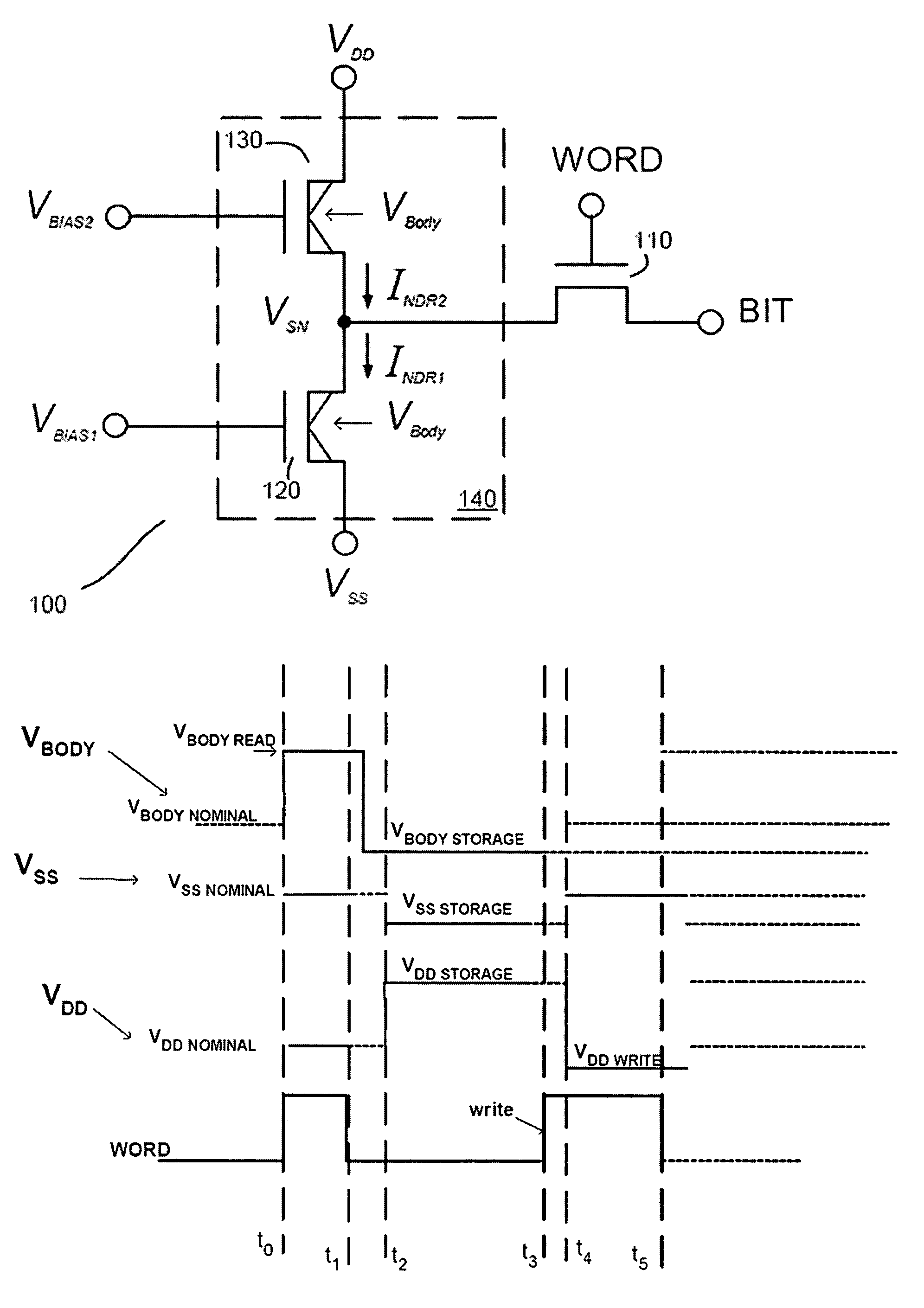
[0030]As noted earlier, FIG. 1 is a circuit diagram of a preferred embodiment of a static memory (SRAM) cell 100 consisting of two NDR elements 120 and 130 that form a bistable latch 140 and one enhancement-mode IGFET access element 110. While a three (3) element implementation is shown in FIG. 1, the invention is by no means limited to such embodiments, as other designs employing NDR elements can also benefit from the present teachings. Within cell 100 NDR element 120 can be considered a pull-down element, or a driver element, while NDR element 130 can be considered as a pull-up element, or a load element as those terms are understood in this field of art.

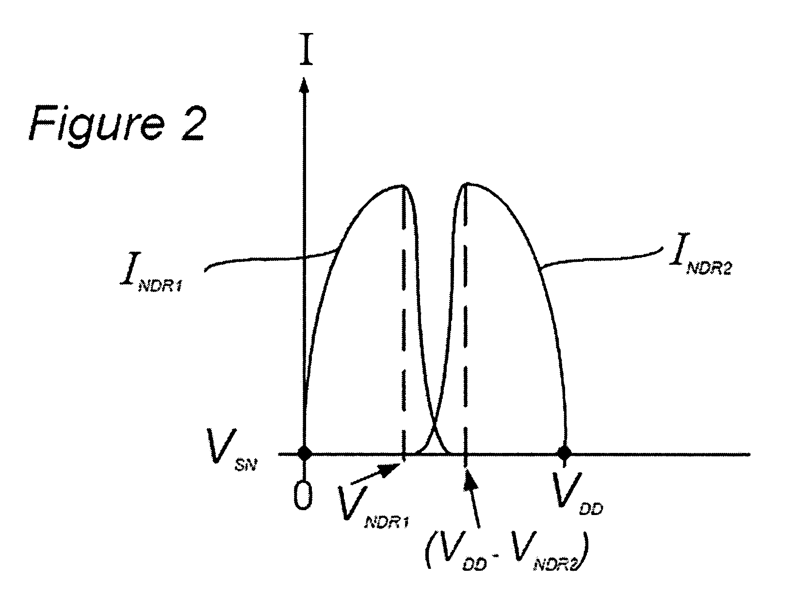
[0031]FIG. 2 is a current-vs.-voltage plot illustrating the general operational characteristics of the static memory cell 100 of FIG. 1, including in a storage mode of operation. Again, it will be understood by those skilled in the art that this Figure is merely intended...


PUM


Abstract

Static random access memory (SRAM) performance is enhanced through the use of appropriate latch strength control. For example, latch strength in an SRAM cell is increased during data store operations to reduce power dissipation and improve reliability. Latch strength can also be increased to improve read speed, while latch strength can be reduced to improve write speed. In an SRAM cell including at least a negative differential resistance (NDR) device as a pull-up element, this type of latch control can be achieved through appropriate biasing of the NDR device(s). For example, drain-to-source bias can be increased or decreased to increase or decrease, respectively, latch strength. Similarly, gate-to-source bias can be increased or decreased to increase or decrease, respectively, latch strength.

Description

REFERENCE TO RELATED APPLICATIONS[0001]This application is a continuation-in-part of U.S. patent application Ser. No. 11 / 010,132 entitled “Enhanced Read And Write Methods For Negative Differential Resistance (NDR) Based Memory Device” filed Dec. 9, 2004, now U.S. Pat. No. 7,012,842, which is a continuation of U.S. patent application Ser. No. 10 / 185,247 entitled “Enhanced Read And Write Methods For Negative Differential Resistance (NDR) Based Memory Device” filed Jun. 28, 2002, now U.S. Pat. No. 6,847,562.FIELD OF THE INVENTION[0002]This invention generally relates to methods of operating semiconductor memory devices and technology, and in particular to biasing operations for memory devices, and particularly static random access memory (SRAM) devices that utilize negative differential resistance (NDR) elements.BACKGROUND OF THE INVENTION[0003]A new type of SRAM device using Negative Differential Resistance Field Effect Transistors (NDR FETs) is described in detail in a patent applica...

Claims


Application Information

Patent Timeline
Patent Type & Authority Patents(United States)
IPC IPC(8): G11C5/14
CPCG11C11/413G11C11/39
Inventor KING, TSU-JAE
Owner SYNOPSYS INC
Why Eureka
Try Eureka