Method and apparatus for efficiently locating and automatically correcting certain violations in a complex existing circuit layout

a technology of complex existing circuits and layouts, applied in computer aided design, program control, instruments, etc., can solve the problems of reducing the reliability of the system, reducing the risk of via failure, and requiring a very intensive design effort for detailed design layouts.

Active Publication Date: 2006-08-22
ORACLE INT CORP
View PDF48 Cites 49 Cited by
  • Summary
  • Abstract
  • Description
  • Claims
  • Application Information

AI Technical Summary

Benefits of technology

[0012]In a deep sub micron semiconductor design, vacancy concentration sometimes causes a higher failure rate on single vias which are located at the center part of a wide landing metal or covering metal geometry, known as an isolated via. It has been observed that putting some extra vias (known as redundant vias) between the same landing and covering metal as the isolated via, results in the vias sharing the vacancy load, so the risk of via failure is reduced and reliability is enhanced. Vias which are close together and vias which are close to the edge of the metal geometry may also benefit from alteration of the stress gradients responsible for vacancy transport, and likewise reduce the risk of via failure. In other words, this type of failure can be substantially reduced by adding a (redundant) via next to the pre-existing (isolated) via or putting the via close to the metal edge. This implementation can be done relatively easily for a new design layout. However, for an existing large scale layout, it is extremely difficult and, in many cases, not practical.

Problems solved by technology

The detailed design layout requires a very intensive and time-consuming design effort and is typically performed utilizing specialized computer aided design (CAD) or Electronic Design Automation (EDA) tools.
DRC is a time-consuming iterative process that often requires manual manipulation and interaction by the designer.
Creation of a design layout and performing DRC become critical time consuming processes.
However, for an existing large scale layout, it is extremely difficult and, in many cases, not practical.

Method used


Image

  • Method and apparatus for efficiently locating and automatically correcting certain violations in a complex existing circuit layout
  • Method and apparatus for efficiently locating and automatically correcting certain violations in a complex existing circuit layout
  • Method and apparatus for efficiently locating and automatically correcting certain violations in a complex existing circuit layout

Examples


Embodiment Construction

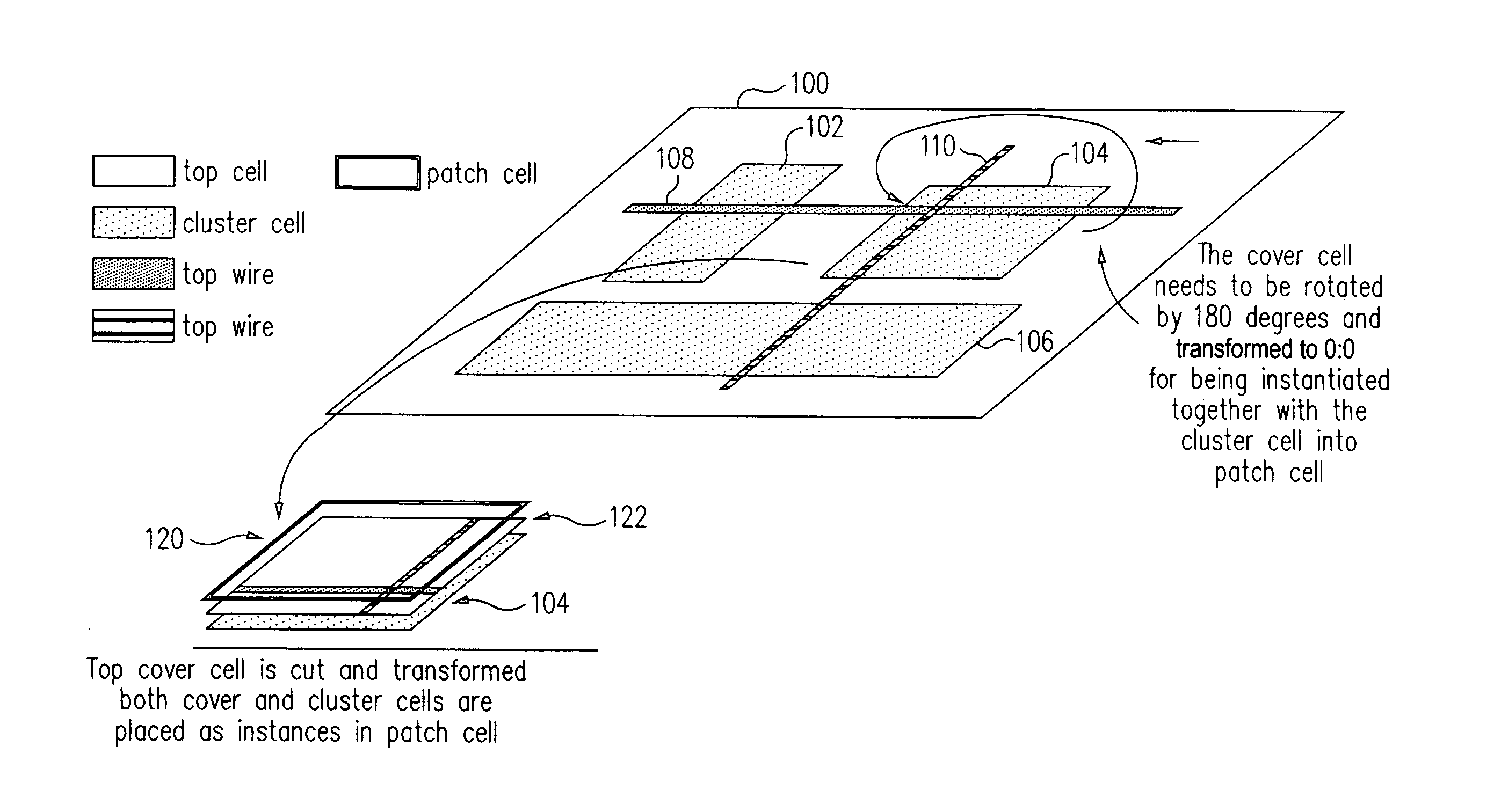
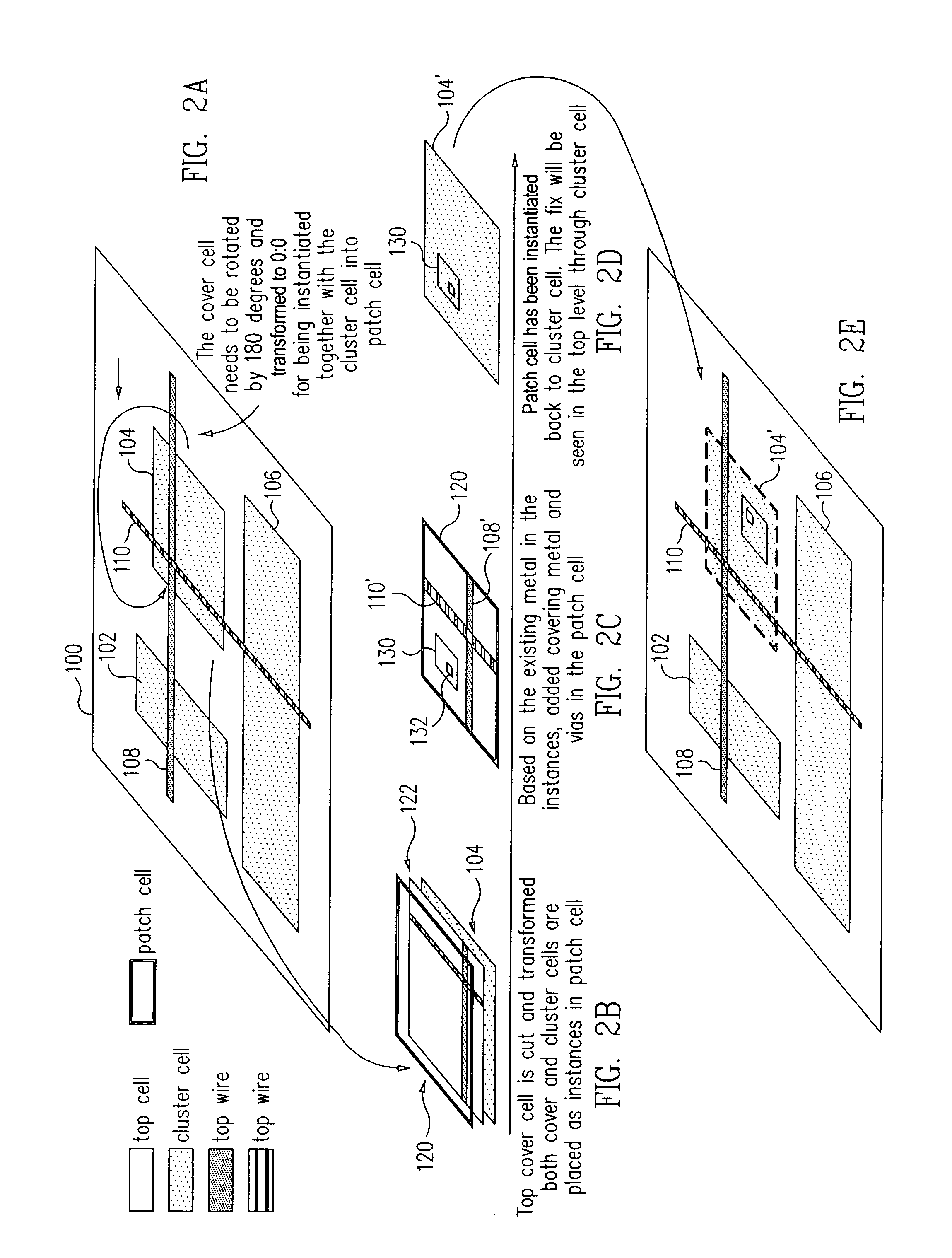
[0021]In many design flows, Electronic Design Automation (EDA) functions are used to extract Pure Fill Via Areas (PFVA) for each metal layer. A PFVA is an artificial object or geometry, which has been pre-shrunk from the original geometry by the correct enclosure amount, which depends on whether the PFVA is within a wide metal area or not. A via can be dropped (i.e., placed) anywhere within such a PFVA without violating the respective via metal enclosure rules. A Layer Pure Fill Via Area (LPFVA) is an area which meets the metal enclosure rule for the specific metal layer. In other words, a via can be placed anywhere inside the area without violating the specific metal enclosure design rule for any wide class. A vx PFVA is the common area of a mtx LPFVA and a mtx+1 LPFVA. In this common area, a vx via meets metal enclosure design rules for both metal layers mtx and mtx+1 anywhere. A LPFVA may be used for filling vias into the area without violating a specific metal layer enclosure de...


PUM


Abstract

An exemplary CAD design flow modifies an existing large scale chip layout to reinforce the redundant via design rules to improve the yield and reliability. The flow operates on each metal-via pair from bottom up to locate and correct isolated via rule violations by adding metal features and vias in a respective patch cell associated with each cluster cell. A large complex design is thus divided into cells so that multiple processes can work concurrently as if every process were working on the top level of the design layout.

Description

BACKGROUND[0001]1. Field of the Invention[0002]The present invention relates to error checking and manipulation of a design layout, and more particularly to computer aided design layout and design rule verification of an integrated circuit design layout, and use thereof for circuit fabrication.[0003]2. Background of the Invention[0004]Design of an electronic circuit, for example, an integrated circuit (IC), is a complicated and time consuming process. FIG. 1 illustrates a typical design flow 80 of an integrated circuit device from conception through the generation of a fabrication ready design layout. Generally, design flow 80 commences with defining the design specifications or requirements, such as required functionality and timing, at step 82. The requirements of the design are implemented, for example, as a netlist or electronic circuit description, at step 84. The implementation can be performed by, for example, schematic capture (drawing the design with a computer aided design...

Claims


Application Information

Patent Timeline
Patent Type & Authority Patents(United States)
IPC IPC(8): G06F17/50
CPCG06F17/5081G06F30/398
Inventor LI, MU-JINGMATURI, SURYANARAYANA R.DIXIT, PANKAJ
Owner ORACLE INT CORP
Why Eureka
Try Eureka