Methods for enhancing capacitors having roughened features to increase charge-storage capacity

a capacitor and feature enhancement technology, applied in capacitors, solid-state devices, instruments, etc., can solve the problems of reducing the storage capacity of dram capacitors, unable to store data reliably, and shrinking the size of dram capacitors, so as to enhance the structural integrity of the semiconductor structure, increase the surface area, and the capacitance of the capacitors

Inactive Publication Date: 2006-09-05
MICRON TECH INC
View PDF84 Cites 2 Cited by
  • Summary
  • Abstract
  • Description
  • Claims
  • Application Information

AI Technical Summary

Benefits of technology

[0008]An illustrative aspect of the present invention includes a semiconductor structure with a rough surface having protrusions formed from an undoped silicon film. If the semiconductor structure is a capacitor, the protrusions help to increase the surface area of one of the electrodes of the capacitor, and hence, the capacitance of the capacitor. The semiconductor structure also includes a polycrystalline surface abutting the rough surface. The polycrystalline surface helps to enhance the structural integrity of the semiconductor structure should perforations exist in the rough surface.

Problems solved by technology

Unfortunately, leakage and depletion often prevent DRAM manufacturers from shrinking the size of a DRAM-cell capacitor from its present size.
But unfortunately, the storage capacity of a DRAM capacitor can be reduced only so much before the DRAM cell can no longer hold its state between refresh cycles, and thus can no longer store data reliably.
Furthermore, conventional electrode material, such as polysilicon, often causes the access speed of a DRAM cell to be relatively slow.
Therefore, because this resistance is effectively in series with the DRAM capacitor, it causes the time constant for charging / discharging the capacitor to be relatively large, and thus causes the DRAM cell to have a relatively long read / write time.
Additionally, conventional barrier materials often prevent manufacturers from reducing the dimensions of a structure disposed in a barrier layer.
But unfortunately, tungsten silicide crystallizes at about 800° C. and forms relatively large grains.
That is, if the structure's width is about the same as or is less than the grain size, tungsten silicide often cannot be used.
Furthermore, although it can sometimes be used as such a barrier layer, titanium nitride oxidizes easily, and thus is unsuitable for use in many applications.
Moreover, conventional electrode materials may cause a circuit coupled to an antifuse to have a relatively slow access speed.
Unfortunately, the relatively high resistance of conventional electrode materials may cause a blown antifuse to have a relatively high resistance.
Because the circuit coupled to the antifuse often has a parasitic capacitance associated therewith, the relatively large time constant of the coupled antifuse electrodes and parasitic capacitance can cause the circuit to have a relatively slow access speed.

Method used


Image

  • Methods for enhancing capacitors having roughened features to increase charge-storage capacity
  • Methods for enhancing capacitors having roughened features to increase charge-storage capacity
  • Methods for enhancing capacitors having roughened features to increase charge-storage capacity

Examples


Embodiment Construction

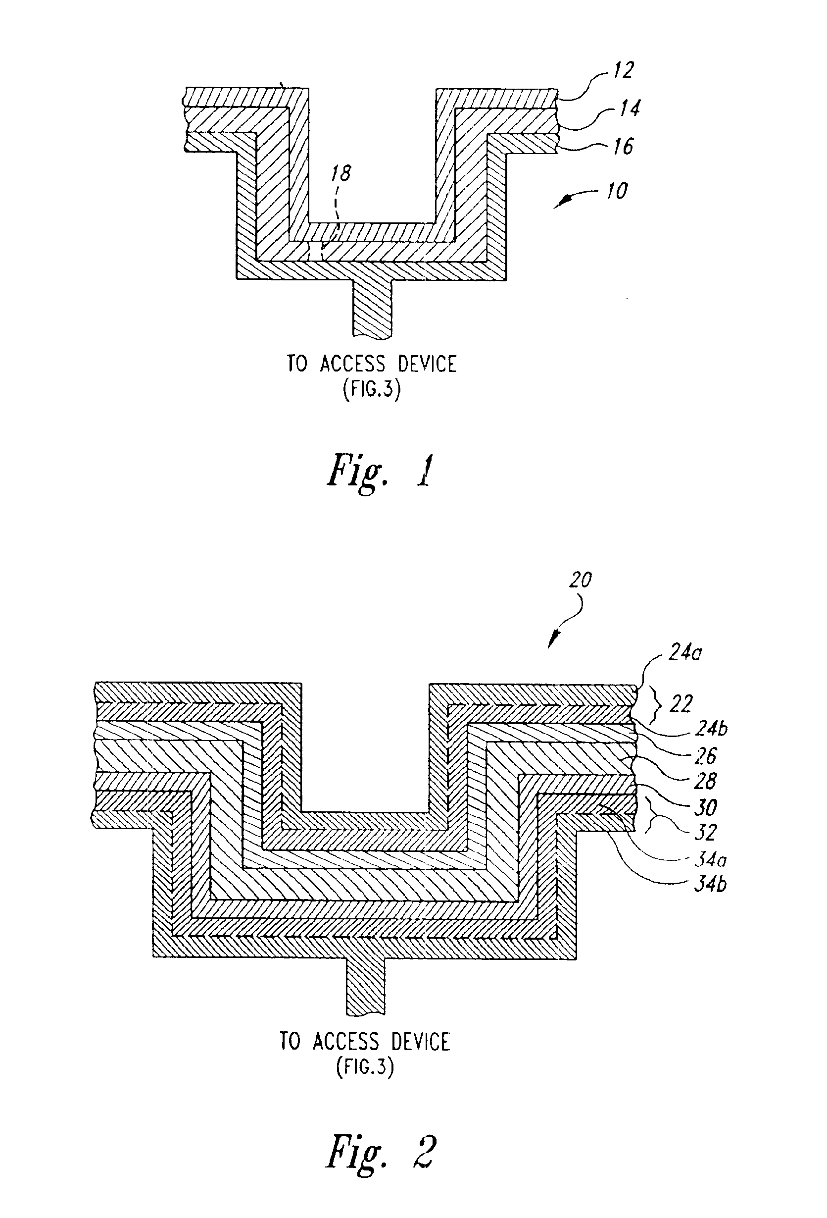
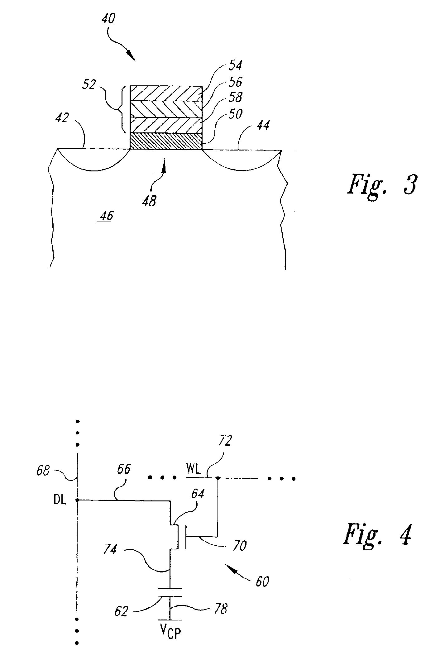
[0020]FIG. 1 is a cross-sectional view of a DRAM capacitor 10 according to one embodiment of the invention. The capacitor 10 includes a conventional electrode 12, which is formed from a conductive material such as polysilicon. The electrode 12 is adjacent to one side of a conventional dielectric 14, which is formed from an insulator such as silicon dioxide, barium strontium titanate, or tantalum pentaoxide. Another electrode 16 is adjacent to another side of the dielectric 14, and is coupled to a DRAM-cell access device, such as a transistor. The electrode 16 is formed from a barrier material, and thus may be called a barrier electrode. The barrier electrode 16 may include conventional barrier materials, such as titanium nitride, or may include tungsten nitride, tungsten silicon nitride, or titanium silicon nitride, which are discussed below in conjunction with FIG. 3. Furthermore, although described for use in a DRAM cell, the capacitor 10 can be used for other applications and in ...


PUM


Abstract

Structures and methods for making a semiconductor structure are discussed. The semiconductor structure includes a rough surface having protrusions formed from an undoped silicon film. If the semiconductor structure is a capacitor, the protrusions help to increase the capacitance of the capacitor. The semiconductor structure also includes a relatively smooth surface abutting the rough surface, wherein the relatively smooth surface is formed from a polycrystalline material.

Description

CROSS-REFERENCE TO RELATED APPLICATIONS[0001]This application is a divisional of pending U.S. patent application Ser. No. 09 / 965,240, filed Sep. 26, 2001, which is a continuation-in-part of U.S. Pat. application Ser. No. 09 / 692,897, filed Oct. 19, 2000, issued Jan. 27, 2004 as U.S. Pat. No. 6,682,970, which is a divisional of U.S. patent application Ser. No. 09 / 260,995, filed Mar. 1, 1999, issued May 1, 2001 as U.S. Pat. No. 6,225,157, which is a divisional of U.S. patent application Ser. No. 09 / 032,182, filed Feb. 27, 1998, issued Nov. 21, 2000 as U.S. Pat. No. 6,150,706. Other related patents include U.S. Pat. No. 5,969,983, issued Oct. 19, 1999, which is a divisional of U.S. Pat. No. 6,150,706; U.S. Pat. No. 6,479,854, issued Nov. 12, 2002, which is a divisional of U.S. Pat. No. 6,150,706; U.S. Pat. No. 6,392,284, issued May 21, 2002, which is a divisional of U.S. Pat. No. 6.150,706; and U.S. Pat. No. 6,541,811, which is a continuation of U.S. Pat. No. 6,682,970.TECHNICAL FIELD[0...

Claims


Application Information

Patent Timeline
Patent Type & Authority Patents(United States)
IPC IPC(8): H01L21/8242H01L21/20H01L21/336G11C11/404G11C17/16H01L21/02H01L21/285H01L21/768H01L21/8246H01L27/115
CPCG11C11/404G11C17/16H01L28/84H01L27/11502H01L27/11507H01L28/82H01L27/10852H01L21/28568H01L21/76888H01L27/1085H01L28/60H10B12/03H10B12/033H10B53/00H10B53/30H01L31/119
Inventor THAKUR, RANDHIR P. S.MERCALDI, GARRY A.NUTTALL, MICHAELCHEN, SHENLINPING, ER-XUAN
Owner MICRON TECH INC
Why Eureka
Try Eureka