Interface device and information processing system

a technology of information processing system and interface device, which is applied in the direction of pulse technique, program control, instruments, etc., can solve the problems of system not being formed on the same semiconductor substrate, incorrect information cannot be transmitted to the signal processing device, and large current consumption

Inactive Publication Date: 2006-09-05
HITACHI LTD
View PDF14 Cites 30 Cited by
  • Summary
  • Abstract
  • Description
  • Claims
  • Application Information

AI Technical Summary

Benefits of technology

[0007]A first object of the invention is to make it possible to propagate a state signal, whose signal level does not change or changes slowly, between the primary side and the secondary side electrically insulated from each other by a capacitor-type insulating circuit.
[0008]A second object of the invention is to provide an interface device having a power supply circuit of low power consumption in order to relax the limitation of the number of the devices connected to the network.
[0009]A third object of the invention is to eliminate the effect of the variations of the substrate potential on the MOS transistor of high breakdown voltage.
[0011]By propagating the state signal in this way, the diagnosis and control operation become possible between areas electrically insulated from each other, thereby making it possible to improve the safety and economy of devices and systems.
[0012]In order to achieve the second object, a network transceiver and a switching regulator are formed on the same semiconductor substrate. The switching regulator, due to the large power noise generated by it, is not normally formed on the same semiconductor substrate as other logic circuits. By limiting the supply current or appropriately designing a circuit for relaxing the switching noise, however, the switching regulator can be formed on the same semiconductor substrate as other logic circuits. In the prior art, the switching regulator and the logic circuits are not advantageously formed on the same semiconductor substrate in this way. In connecting a plurality of devices to a network, however, the number of the devices to be connected is limited by the power consumption per device. Of the devices connected to the network, therefore, the network transceiver and the switching regulator are formed on the same semiconductor substrate, thereby making it possible to increase the number of devices connectable to the network. The switching regulator and the network transceiver can be mounted as independent parts on the board. In such a case, however, the mounting area is increased on the one hand, and a noise is generated by the resistance and inductance added to the power lines by the wire and bonding for connecting the parts on the other hand. By forming the network transceiver and the switching regulator on the same semiconductor substrate, the function of monitoring the state of the power supply can be shared with the power supply circuit and therefore the circuit can be reduced in size.

Problems solved by technology

This system, however, poses the problem that the current consumption is large and the system cannot be formed on the same semiconductor substrate as the peripheral circuit.
Since the power supply circuit on the primary side of the network devices is out of order, on the other hand, correct information cannot be transmitted to the signal processing device on the secondary side, and in the worst case, the system is unavoidably stopped.
In the capacitor-type insulating system, however, the output of the power supply circuit cannot be transmitted as it is as a state signal, since what is called the differential transmission system is used in which the change portion of the signal is transmitted.
In an interface device using the capacitor-type insulating system, therefore, the state signal cannot be transmitted, so that the status of the power supply circuit cannot be transmitted to the secondary side.
Secondly, the prior art consumes the power of the power supply circuit in a great amount, which poses a problem regardless of whether the devices are insulated or not.
The power consumption, even though negligible for a single device, reaches an amount that cannot be ignored in a network connection.
An increased power consumption increases the load on the network power supply, and the number of devices exceeding the power supply capacity cannot be connected.
In other words, the problem is that the number (N) of the devices that can be connected to the network is limited.
A floating substrate potential, therefore, poses the problem that the operation of the MOS transistor of high breakdown voltage becomes unstable.

Method used


Image

  • Interface device and information processing system
  • Interface device and information processing system
  • Interface device and information processing system

Examples


Embodiment Construction

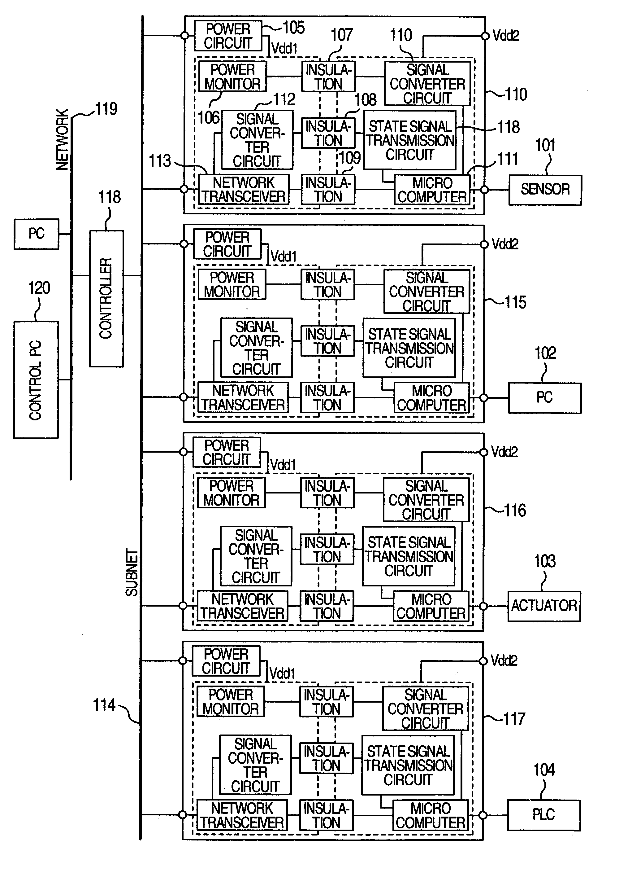
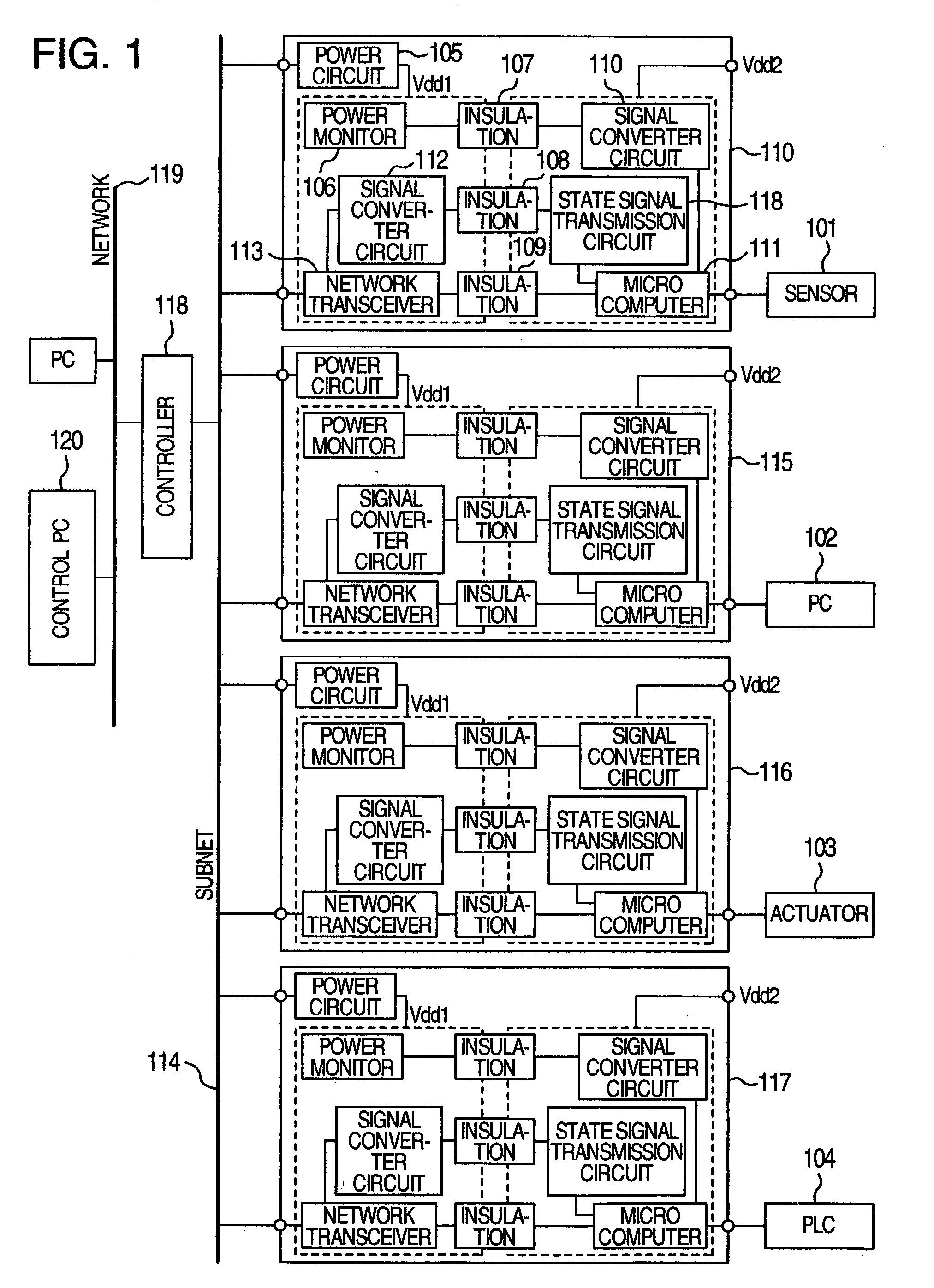
[0025]FIG. 1 shows a distributed control system according to this invention. In this distributed control system, various field devices including a sensor 101, a personal computer (PC) 102, an actuator 103 and a programmable logic controller (PLC) 104 are connected to a network 114 through interface devices 100, 115, 116, 117. The interface devices 100, 115, 116, 117 may be formed independently of the sensor 101, the personal computer 102, the actuator 103 and the programmable logic controller 104, respectively, or each field device may have an interface device built therein. The network 114 is further connected through a controller 118 to a higher-order network 119 connected with a control personal computer (control PC) 120 and the like. In addition to the configuration of the distributed control system described above, various system configurations are possible according to the hierarchy and type of the network.

[0026]In the distributed control system configured in this way, the who...


PUM


Abstract

A first converter circuit converts a state signal, whose level is constant or slowly varies during a predetermine period of time, into a pulse signal to allow the signal to propagate across an electrically insulating area. A second converter circuit converts the pulse signal, which has propagated through an insulating circuit, into the original state signal or a signal having the same characteristics as the original state signal.

Description

[0001]This application is a continuation of application Ser. No. 10 / 149,763, filed Jun. 13, 2002 now U.S. Pat. No. 6,977,522, which is a 371 of PCT / JP99 / 07041, filed Dec. 15, 1999.TECHNICAL FIELD[0002]The present invention relates to an interface device connected between, for example, a network and an information processing system such as a personal computer or a controller.BACKGROUND ART[0003]Conventionally, an insulating system using a photocoupler is used for electrical insulation. This system, however, poses the problem that the current consumption is large and the system cannot be formed on the same semiconductor substrate as the peripheral circuit. A capacitor-type insulating system is described in JP-A-11-252270 as an insulating system which is smaller in current consumption and can be formed on the same semiconductor substrate as the peripheral circuit. The capacitor-type insulating system is configured of a filter including a capacitor and a resistor for cutting off the sig...

Claims


Application Information

Patent Timeline
Patent Type & Authority Patents(United States)
IPC IPC(8): H03K19/0175G05B19/042G06F3/00H01L21/762H01L27/06
CPCG05B19/0428H04L25/0266H01L21/76283H01L27/0629G05B2219/25428G05B2219/25462G06F3/00
Inventor MURABAYASHI, FUMIOSASE, TAKASHIKIKUCHI, MUTSUMIWATANABE, ATSUOAMISHIRO, MASATSUGUTABUCHI, KENJI
Owner HITACHI LTD
Why Eureka
Try Eureka