High-electron mobility transistor with zinc oxide

a high-electron mobility, zinc oxide technology, applied in the direction of electrical apparatus, semiconductor/solid-state device manufacturing, semiconductor devices, etc., can solve the problems of affecting the mobility, cracking of the film, and less familiar semiconductor materials that cannot penetrate higher-power high-frequency applications to the extent desirable, and achieve the effect of high-electron mobility

Inactive Publication Date: 2006-09-12
NAUSE CATHERINE D
View PDF23 Cites 3950 Cited by
  • Summary
  • Abstract
  • Description
  • Claims
  • Application Information

AI Technical Summary

Benefits of technology

[0011]According to one embodiment of the present invention, there is provided a FET comprising a channel layer composed of ZnO grown homoepitaxially on a semi-insulating ZnO substrate. A gate contact is disposed on the channel layer. A gate insulating layer is disposed between the gate contact and the channel layer and is composed o

Problems solved by technology

These more familiar semiconductor materials have failed to penetrate higher power high frequency applications to the extent desirable, however, because of their relatively small bandgaps (e.g., 1.12 eV for Si and 1.42 eV for GaAs at room temperature) and relatively small breakdown voltages.
When MgZnO

Method used


Image

  • High-electron mobility transistor with zinc oxide
  • High-electron mobility transistor with zinc oxide
  • High-electron mobility transistor with zinc oxide

Examples


Embodiment Construction

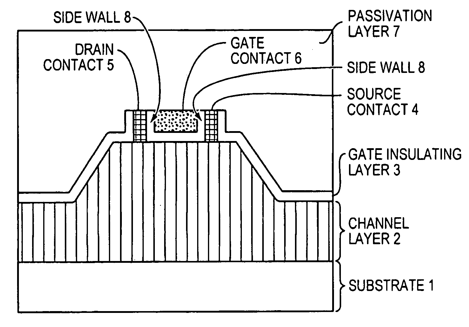
[0019]FIG. 1 illustrates the configuration of the HEMT according to the first embodiment of the present invention. In this HEMT, a channel layer 2 and a gate insulating layer 3 are sequentially laminated on a ZnO substrate (for example, a c-surface substrate). Formed on the gate insulating film 3 are a source electrode 4, which is electrically connected to the channel layer 2 via an opening of the gate insulating layer 3. Further, a gate electrode 6 is disposed on the gate insulating layer 3 having side walls 8. The source contact 4, the drain contact 5, and the gate contact 6 are formed by sequentially laminating from the upper surface of the substrate 1. The substrate is formed from high resistance insulating ZnO. The channel layer 2 is made from n-type ZnO doped with an n-type impurity, such as gallium, and has a thickness, for example, 0.1 micrometer. The concentration of the n-type impurity is, for example, 1018 atoms per cubic centimeter (cm3). The impurity concentration and t...


PUM


Abstract

A zinc oxide (ZnO) field effect transistor exhibits large input amplitude by using a gate insulating layer. A channel layer and the gate insulating layer are sequentially laminated on a substrate. A gate electrode is formed on the gate insulating layer. A source contact and a drain contact are disposed at the both sides of the gate contact and are electrically connected to the channel layer via openings. The channel layer is formed from n-type ZnO. The gate insulating layer is made from aluminum nitride/aluminum gallium nitride (AlN/AlGaN) or magnesium zinc oxide (MgZnO), which exhibits excellent insulation characteristics, thus increasing the Schottky barrier and achieving large input amplitude. If the FET is operated in the enhancement mode, it is operable in a manner similar to a silicon metal oxide semiconductor field effect transistor (Si-MOS-type FET), resulting in the formation of an inversion layer.

Description

CROSS-REFERENCE TO RELATED APPLICATION[0001]This patent application is a U.S. nonprovisional application filed pursuant to Title 35, United States Code §§100 et seq. and 37 C.F.R. Section 1.53(b) claiming priority under Title 35, United States Code §119(e) to U.S. provisional application no. 60 / 391,519 filed Jun. 24, 2002 naming Jeffrey E. Nause and Shanthi Ganesan as inventors. Both the subject application and its provisional application have been or are under obligation to be assigned to the same entity.BACKGROUND OF THE INVENTION[0002]1. Field of the Invention[0003]The present invention relates to a high electron mobility transistor (HEMT). More particularly, the present invention relates to a HEMT formed as a field effect transistor (FET) having a gate insulating layer positioned between a gate contact and channel layer. The invention also pertains to manufacturing methods for the aforementioned HEMT device.[0004]2. Description of the Related Art[0005]As known to those familiar ...

Claims


Application Information

Patent Timeline
IPC IPC(8): H01L31/0328H01L29/20H01L29/22H01L29/267H01L29/778
CPCH01L29/7786H01L29/267H01L29/22H01L29/2003
Inventor NAUSE, JEFFGANESAN, SHANTHI
Owner NAUSE CATHERINE D
Why Eureka
Try Eureka