Semiconductor device and method for fabricating same

a technology of semiconductors and semiconductors, applied in the direction of sustainable manufacturing/processing, final product manufacturing, and metal adhesion improvement of insulating substrates, can solve the problem that the above technology cannot be applied to a package of area array types, and achieve the effect of enhancing the adhesion strength between the lead frame and the printed circuit board and high reliability

Inactive Publication Date: 2006-09-19
NEC CORP
View PDF26 Cites 15 Cited by
  • Summary
  • Abstract
  • Description
  • Claims
  • Application Information

AI Technical Summary

Benefits of technology

[0065]assembling the lead frame on which the semiconductor chip is mounted into a printed circuit board by bringing the unevennesses formed on the lead frame into contact with tenth conductive pads formed on the printed circuit board.
[0066]According to the aforementioned structure, since areas of the contact surfaces between the lead frame and the printed circuit board increase, the lead frame becomes hard to exfoliate from the printed

Problems solved by technology

Accordingly, the aforementioned technology canno

Method used


Image

  • Semiconductor device and method for fabricating same
  • Semiconductor device and method for fabricating same
  • Semiconductor device and method for fabricating same

Examples


Embodiment Construction

[0088]Hereafter, preferred embodiments of the invention will be explained.

[The First Preferred Embodiment]

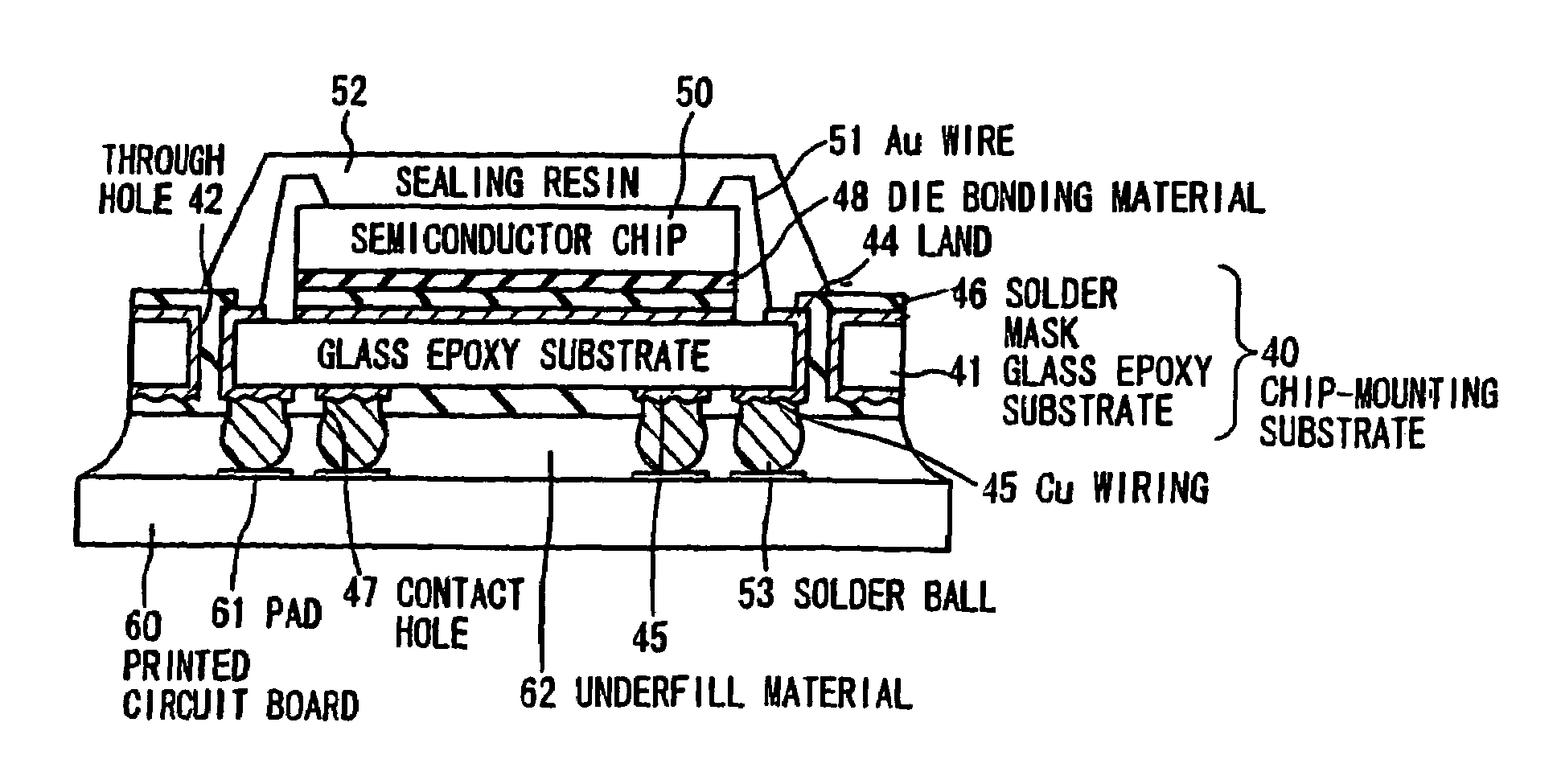
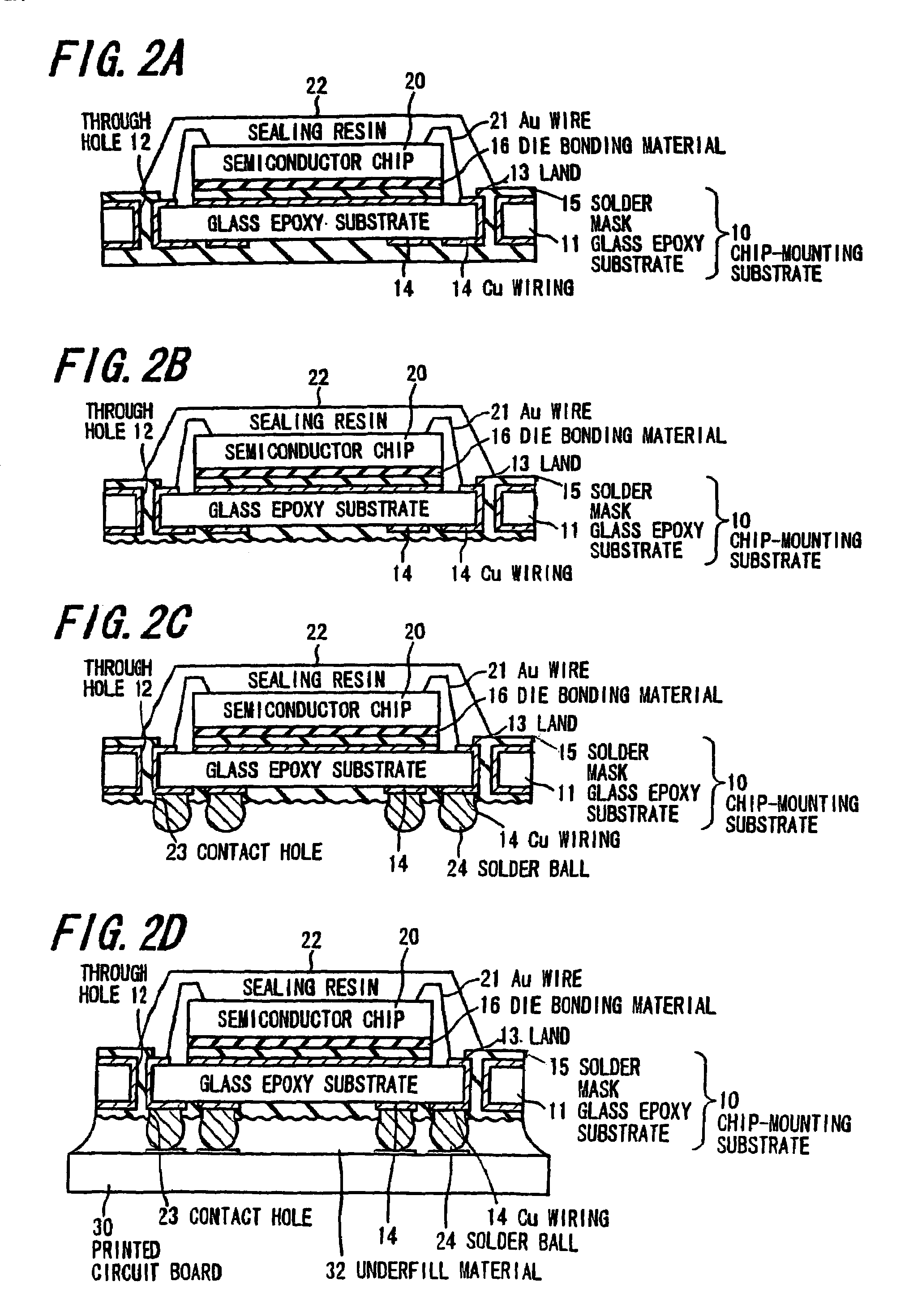
[0089]As shown in FIG. 2D, a semiconductor device according to the first preferred embodiment is fabricated by packaging a semiconductor chip in accordance with CSP (chip scale package), and provided with a chip-mounting substrate 10, semiconductor chip 20, and a printed circuit board 30.

[0090]The chip-mounting substrate 10 is composed of a glass fiber-reinforced epoxy substrate (a glass epoxy substrate, hereinafter) 11 of a single layer which is provided with plural through holes 12 formed on a periphery thereof, lands 13 formed on a top surface of the glass epoxy substrate 11, Cu wirings (pads) 14 which are formed on a bottom surface of the glass epoxy substrate 11 and connected with the lands 13 via the through holes 12, and solder balls 24 formed on the Cu wirings 14. A solder mask 15 is formed on the Cu wirings 14 and the lands 13. Moreover, unevenness is provided for a bot...


PUM


Abstract

Lands and Cu wirings are formed on surfaces of a glass epoxy substrate, and a solder mask is formed on the lands and the Cu wirings to form a chip-mounting substrate. A bottom surface of the chip-mounting substrate is made rough, and a semiconductor chip is mounted on a top surface of the chip-mounting substrate. Through holes communicating with the Cu wirings are formed on the solder mask to expose the Cu wirings. Solder balls are formed on the Cu wrings by thermal compression welding. Underfill material is injected into a clearance formed between the chip mounting substrate and a printed circuit board. Since the surface of the chip-mounting substrate is made rough, an area of a contact surface between the chip-mounting substrate and underfill material increases, hence an adhesive strength between the chip-mounting substrate and the printed circuit board is heightened.

Description

[0001]The present Application is a Division Application of U.S. patent application Ser. No. 09 / 893,791, filed on Jun. 29, 2001 U.S. Pat. No. 6,806,560.FIELD OF THE INVENTION[0002]The invention relates to a semiconductor device and a method for fabricating the same, and especially to a semiconductor device in which a semiconductor chip is assembled into a printed circuit board and a method for fabricating the same.BACKGROUND OF THE INVENTION[0003]In recent years, an electronic device has come to be integrated with high density, and a semiconductor chip with multiple terminals is packaged in accordance with an improvement of the function and thinning of an electronic circuit. Accordingly, a package of the semiconductor chip used in the electronic circuit is miniaturized and provided with multiple pins. In conformity with the aforementioned tendency, the semiconductor chip is assembled into a printed circuit board by means of a package of an area array type, such as a ball grid array p...

Claims


Application Information

Patent Timeline
IPC IPC(8): H01L21/50H01L21/52H01L23/28H01L21/56H01L23/13H01L23/31H01L23/495H01L23/498H01L23/50H05K1/11H05K3/30H05K3/34H05K3/38
CPCH01L21/563H01L23/13H01L23/3121H01L23/3128H01L23/49548H01L23/49816H01L24/32H05K3/305H01L24/29H01L24/45H01L2224/32225H01L2224/32245H01L2224/45144H01L2224/48091H01L2224/48105H01L2224/48227H01L2224/48228H01L2224/48247H01L2224/73203H01L2224/73265H01L2224/83192H01L2224/92247H01L2924/01004H01L2924/01029H01L2924/01047H01L2924/01078H01L2924/01079H01L2924/01082H01L2924/15311H05K1/111H05K3/381H05K2201/10734H05K2201/10977H05K2203/0307H01L2924/01005H01L2924/01006H01L2924/01033H01L24/48H01L2924/00014H01L2924/00H01L2924/3512H01L2924/15787H01L2924/12042H01L2924/181H01L2224/05554H01L2924/10161Y02P70/50H01L2224/2612H01L2924/00012H01L21/52
Inventor KOBAYASHI, YUTAKA
Owner NEC CORP
Why Eureka
Try Eureka