Arrangement and method impedance matching

a technology of impedance matching and arrangement, applied in the field of impedance matching, can solve problems such as degrading pa rf performance deviation

Inactive Publication Date: 2006-09-26
NXP USA INC
View PDF7 Cites 8 Cited by
  • Summary
  • Abstract
  • Description
  • Claims
  • Application Information

AI Technical Summary

Benefits of technology

[0039]requires only standard IC production and test tools
[0041]only a small increase in die size (due to integration of capacitor), but the total size of the solution may be significantly reduced (e.g., by 50%) because of the reduced number of external components.

Problems solved by technology

However, this approach has the disadvantage(s) that the SMD capacitors have, for cost purpose, a poor quality factor which results in losses and a non-negligable series parasitic inductance that narrows the bandwidth, as well as a large tolerance which degrades the PA RF performance deviation over a number of performance parameters.

Method used


Image

  • Arrangement and method impedance matching
  • Arrangement and method impedance matching
  • Arrangement and method impedance matching

Examples


Embodiment Construction

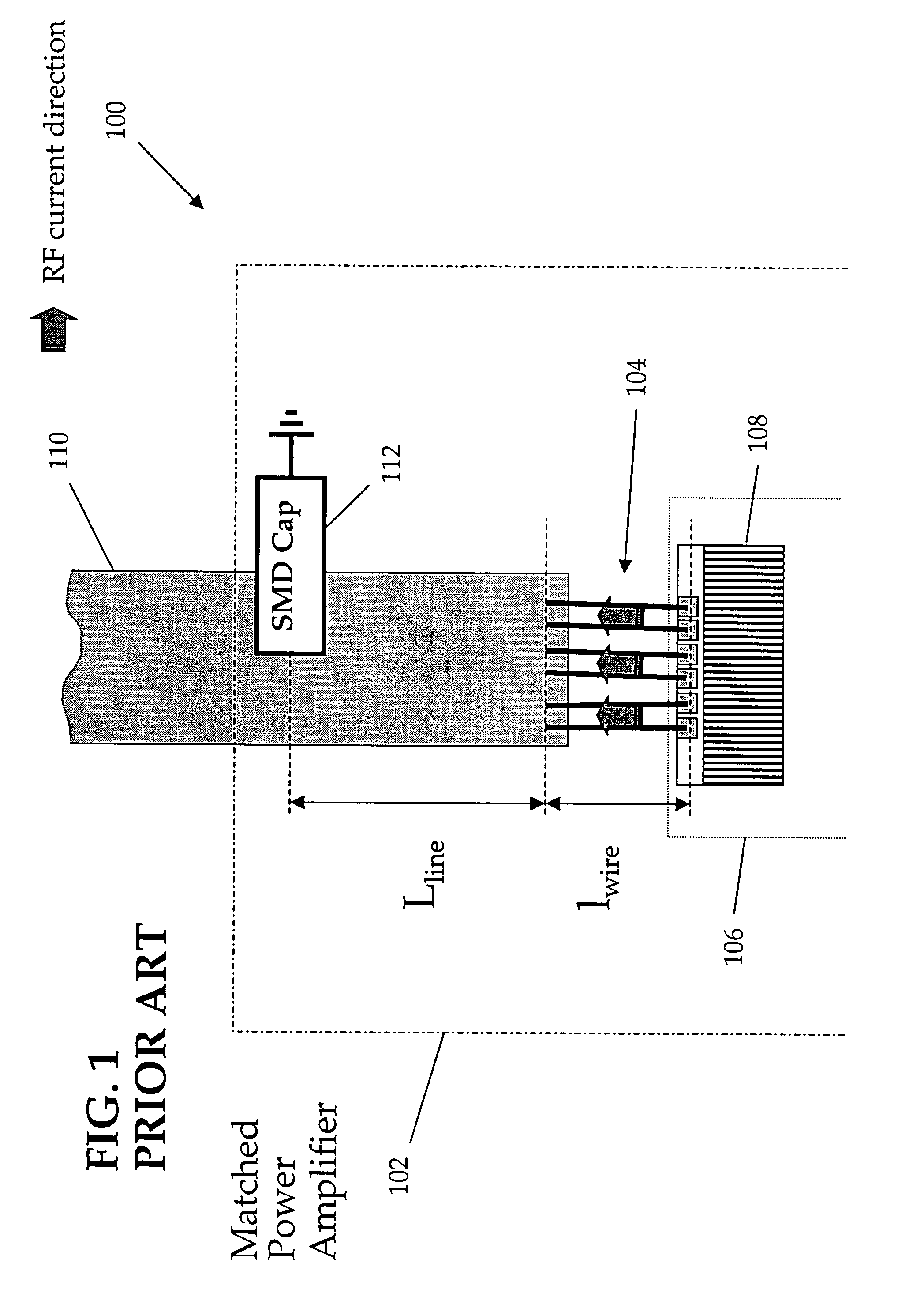
[0015]Referring firstly to FIG. 1, a known impedance matching arrangement 100 for a power amplifier 102 (such as a module dual-band PA for use in cellular radio applications) has a number of wires 104 attached by conventional wire-bonding techniques between an IC 106 with an RF power transistor 108 to be matched and a printed transmission line 110. An external surface-mount device (SMD) capacitor 112 is connected between earth / ground and a precise position on the printed transmission line 110 remote from the wires 104.

[0016]In this arrangement it will be appreciated that the inductor (Llin+1wire) is realised with the printed transmission line 110, the length of which determines the inductance value Lline, and the inductance from the wires which determines the inductance value 1wire. The length of the printed transmission line 110 is defined by the precise position of the SMD capacitor 112. Such an arrangement constitutes a matching cell that increases the output impedance of the RF ...


PUM


Abstract

An arrangement and method for impedance matching (e.g., for a power amplifier) comprising a first node (204a) for receiving an output current to be impedance matched; a second node (212, 214) for receiving output current from the first node; a first current conductor (202c) for carrying current from the first node to the second node; a third node (204b) for receiving output current from the second node; and a second current conductor (202d) for carrying current from said second node to said third node, whereby the first and second current conductors are closely positioned so that their inductance is the sum of their self-inductances and the negative sum of their mutual inductance. The current conductors may be wire bonds, the arrangement may include a capacitor integrated in a power amplifier IC module, in which the capacitor may be provided in a separate IC from the power amplifier, the arrangement may utilise a plurality of impedance matching cells, and the wire bonds may be interdigitated across the semiconductor die. This provides the following advantages: easy to implement; increased accuracy of matching; requires few external components; easy to manufacture; no need for dedicated design flow; requires only standard IC production and test tools; uses low loss matching networks; involves only a small increase in die size (due to integration of capacitor), but the total size of the solution may be significantly reduced (e.g., by 50%) because of the reduced number of external components.

Description

FIELD OF THE INVENTION[0001]This invention relates to impedance matching, and particularly though not exclusively to impedance matching of power amplifiers.BACKGROUND OF THE INVENTION[0002]In the field of this invention it is known that for optimum transfer of energy, from devices such as power amplifiers, the output impedance of the power amplifier should match the input impedance of circuitry driven by the power amplifier. In practice, the output impedance of a power amplifier such as an integrated circuit (IC) power amplifier (PA) is typically matched by use of an electrical / electronic network including components such as inductors and capacitors mounted externally to the IC and connected to the IC by wires. Wire-bonding is typically used to connect the wires. Capacitors may be metal-oxide-semiconductor capacitors (MOSCAPs) or Surface Mounted Device (SMD) capacitors. Inductors are generally made with transmission lines, such as microstrip or coplanar lines, shunted to ground at a...

Claims


Application Information

Patent Timeline
Patent Type & Authority Patents(United States)
IPC IPC(8): H03H7/38H03F3/60H01L23/66H03F1/56
CPCH01L23/66H01L24/49H03H7/383H01L2924/12041H01L2924/01015H01L2924/19107H01L2924/10329H01L2924/01043H01L2224/4911H01L2224/48227H01L24/48H01L2924/3011H01L2924/30107H01L2924/30105H01L2924/19043H01L2924/19042H01L2223/6611H01L2223/6644H01L2224/49111H01L2224/49171H01L2224/49175H01L2924/01005H01L2924/01006H01L2924/01014H01L2924/01031H01L2924/01033H01L2924/01058H01L2924/01074H01L2924/01082H01L2924/14H01L2924/19041H01L2924/00H01L2924/30111H01L2924/00014H01L2224/45099H01L2224/05599H03H11/28
Inventor RIONDET, PHILLIPEMONTORIOL, GILLESTRICHET, JAQUES
Owner NXP USA INC
Why Eureka
Try Eureka