Method for making a carbon nanotube-based field emission display

a carbon nanotube and display device technology, applied in the field of carbon nanotube field emission display devices, can solve the problems of difficult control of the distance between the emitter and the gate electrode, the inability to reliably produce field emission from the bundle of carbon nanotubes, and the inability to precisely control the growth heigh

Active Publication Date: 2006-10-03
TSINGHUA UNIV
View PDF4 Cites 43 Cited by
  • Summary
  • Abstract
  • Description
  • Claims
  • Application Information

AI Technical Summary

Benefits of technology

[0008]Accordingly, an object of the present invention is to provide a method for making a carbon nanotube-based field emission display device wherein a distance between emission tips and gate electrodes is precisely controllable.

Problems solved by technology

These defects usually result in uniformity and unreliability of the field emission from the bundles of carbon nanotubes.
Although the carbon nanotubes array growth higher with longer the reaction time, it is very difficult to control the growth height precisely.
Therefore, the distance between the emitters and the gate electrodes is difficult to control merely by growth.

Method used


Image

  • Method for making a carbon nanotube-based field emission display
  • Method for making a carbon nanotube-based field emission display
  • Method for making a carbon nanotube-based field emission display

Examples


Embodiment Construction

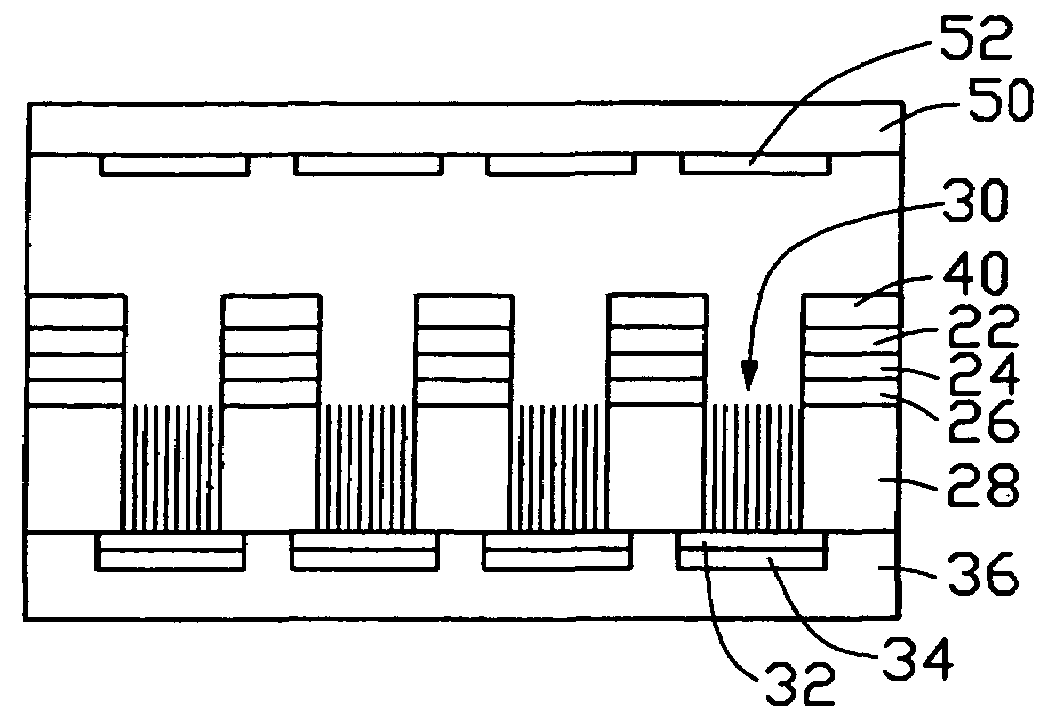
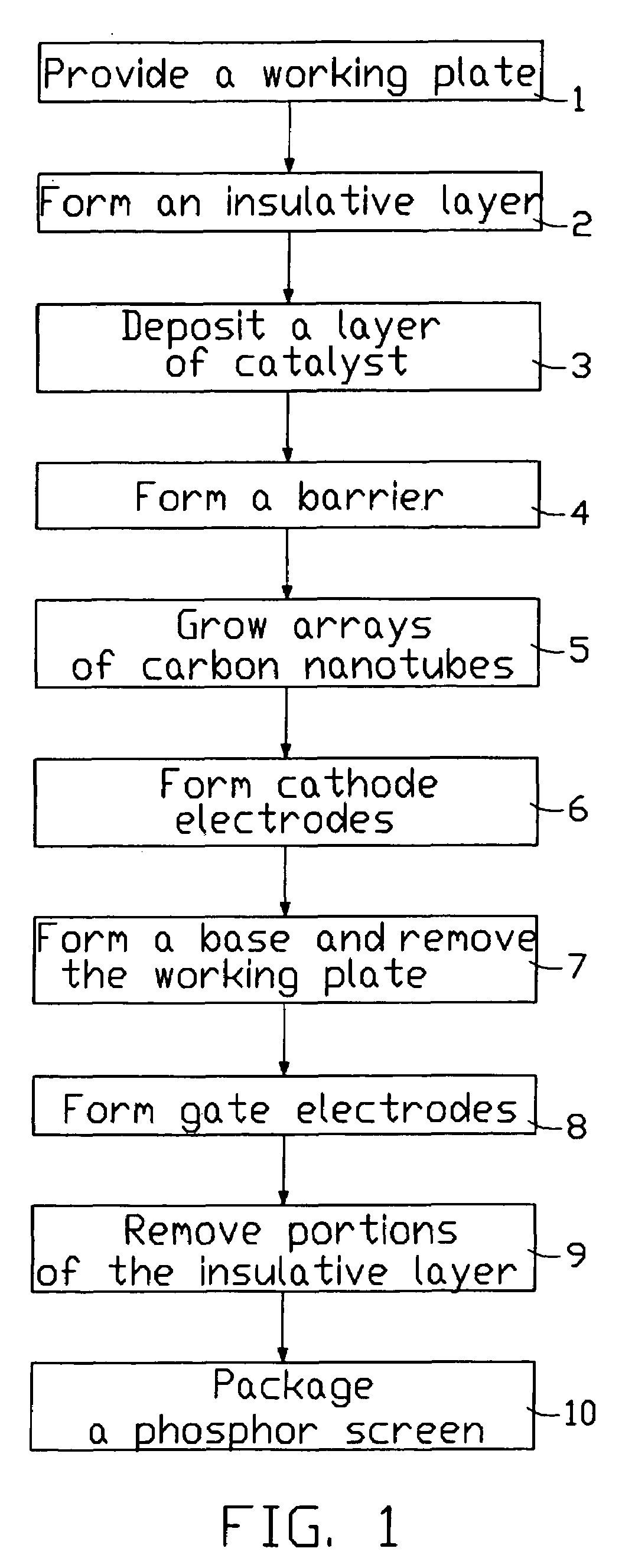
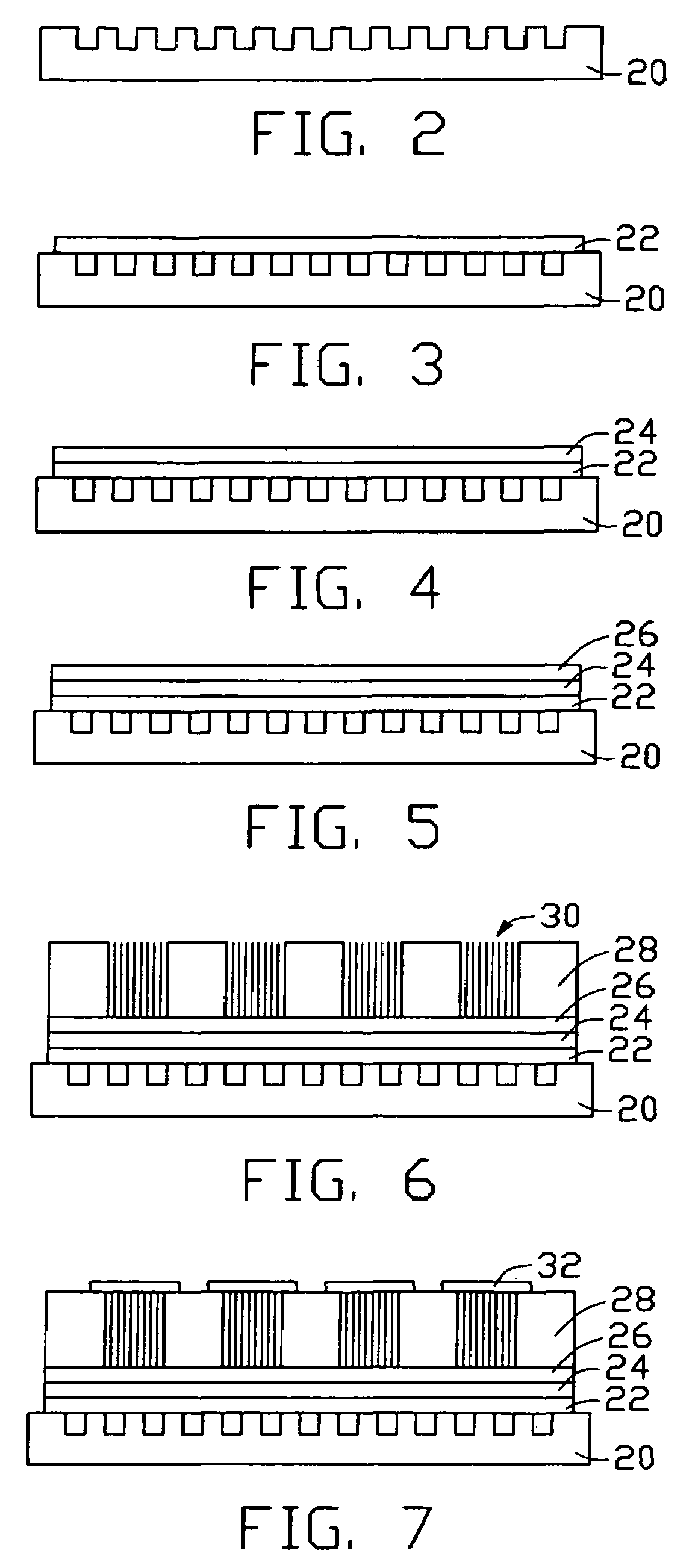
[0024]A preferred method for making a carbon nanotube-based field emission display device in accordance with the invention will be described below with reference to FIG. 1.

[0025]Step 1 is providing a working plate. This is an optional step for the purpose of conveniently carrying out the subsequent steps. The working plate can be a nonmetallic material or a metallic material that is sufficiently heat stable to endure high temperatures at which carbon nanotubes are produced.

[0026]Step 2 is forming an insulative layer on the working plate. The insulative layer is made of insulative material such as silicon oxide, and has a predetermined thickness. In order to form carbon nanotubes from a common surface, a first surface of the insulative layer should be smooth and flat. Preferably, a variation in flatness of the first surface is less than 1 micron.

[0027]Step 3 is depositing a layer of catalyst on the first surface of the insulative layer. Generally, the catalyst is a transition metal s...


PUM


Abstract

A method for making a carbon nanotube-based field emission display device includes the following steps: providing an insulative layer (22) having a first surface; depositing a layer of catalyst (26) on the first surface of the insulative layer; forming a spacer (28) having a number of openings therein such that patterned areas of the layer of catalyst are exposed in the openings; forming arrays of carbon nanotubes (30) extending from the layer of catalyst in the openings; forming a cathode electrode (34) on a top of each of the arrays of carbon nanotubes; forming gate electrodes (40) on a second, opposite surface of the insulative layer offset from the patterned areas; removing portions of the insulative layer corresponding to the arrays of carbon nanotubes so as to expose the arrays of carbon nanotubes; and attaching an anode electrode (50) having a phosphor screen (52) to the above obtained structure.

Description

BACKGROUND OF THE INVENTION[0001]1. Field of the Invention[0002]The present invention relates to a method for making a field emission display device, and more particularly to a method for making a carbon nanotube field emission display device.[0003]2. Description of Prior Art[0004]Carbon nanotubes are a novel carbonaceous material discovered by Iijima, a researcher of NEC corporation, in 1991. Relevant information was reported in an article by Iijima, entitled “Helical Microtubules of Graphitic Carbon” (Nature, Vol. 354, P56, 1991). Carbon nanotubes can transmit an extremely high electrical current and emit electrons easily at a very low voltage of less than 100 volts, which make it a very promising potential material for field emission applications.[0005]Referring to FIG. 13, U.S. Pat. No. 6,232,706, invented by Hongjie Dai et al., discloses a field emission device using aligned parallel bundles of carbon nanotubes 100 extending from patterned catalyst layers 130 deposited on a lay...

Claims


Application Information

Patent Timeline
Patent Type & Authority Patents(United States)
IPC IPC(8): H01J9/00H01J9/04H01J9/02
CPCB82Y10/00H01J9/025H01J2201/30469
Inventor LIU, LIANGFAN, SHOU SHAN
Owner TSINGHUA UNIV
Why Eureka
Try Eureka