Embedded DRAM for metal-insulator-metal (MIM) capacitor structure

Inactive Publication Date: 2006-10-03
TAIWAN SEMICON MFG CO LTD
View PDF20 Cites 17 Cited by
  • Summary
  • Abstract
  • Description
  • Claims
  • Application Information

AI Technical Summary

Benefits of technology

[0007]Another object of the present invention is to provide a method for fabricating a me

Problems solved by technology

In merging logic circuits and dynamic random access memory (DRAM) arrays on a single chip, compatibility is the primary issue with respect to both design and fabrication.
But

Method used


Image

  • Embedded DRAM for metal-insulator-metal (MIM) capacitor structure
  • Embedded DRAM for metal-insulator-metal (MIM) capacitor structure
  • Embedded DRAM for metal-insulator-metal (MIM) capacitor structure

Examples


Embodiment Construction

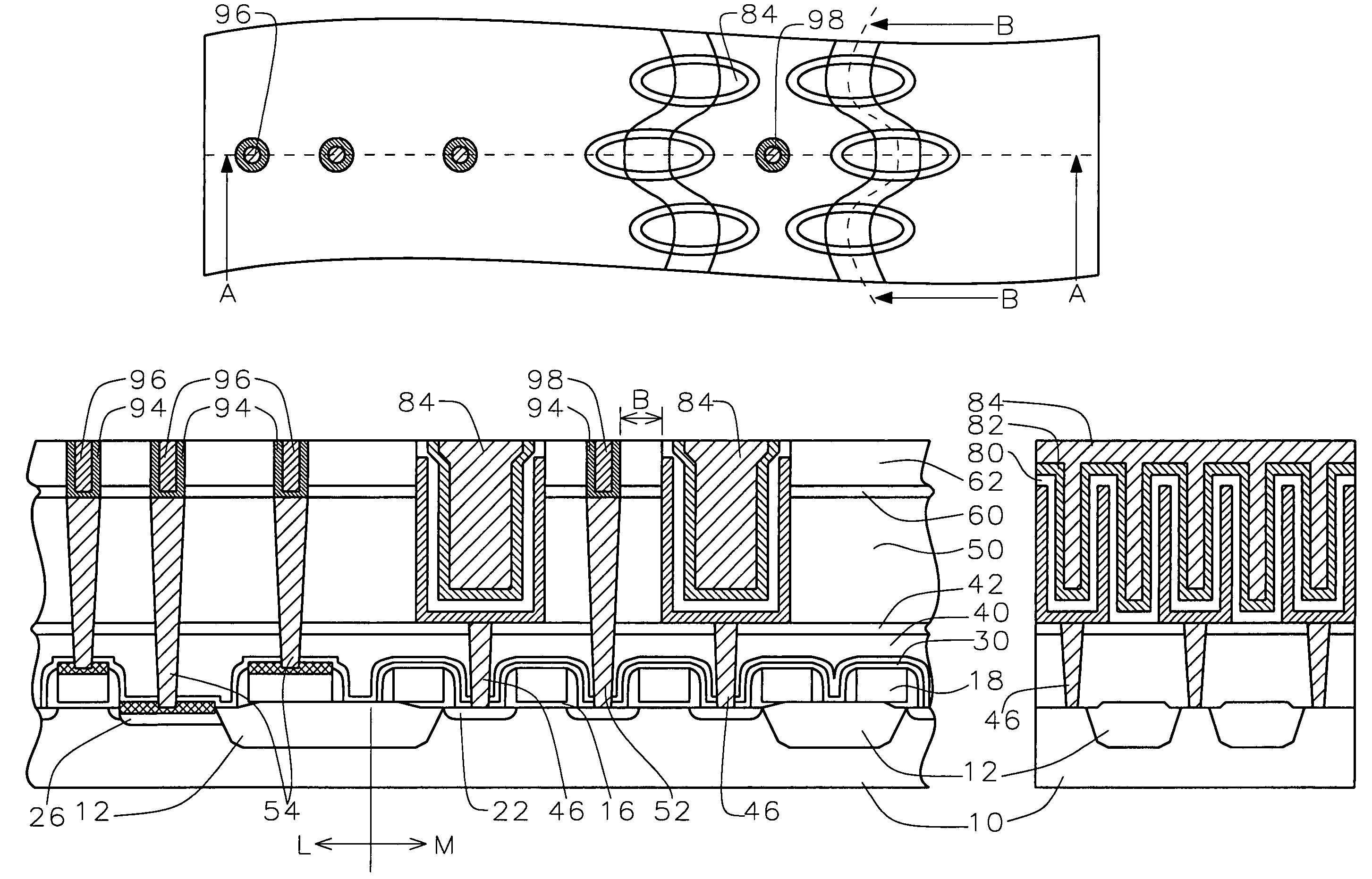
[0017]The process of the present invention provides methods for fabricating a metal-insulator-metal (MIM) capacitor in an embedded DRAM process wherein the contact etch is improved.

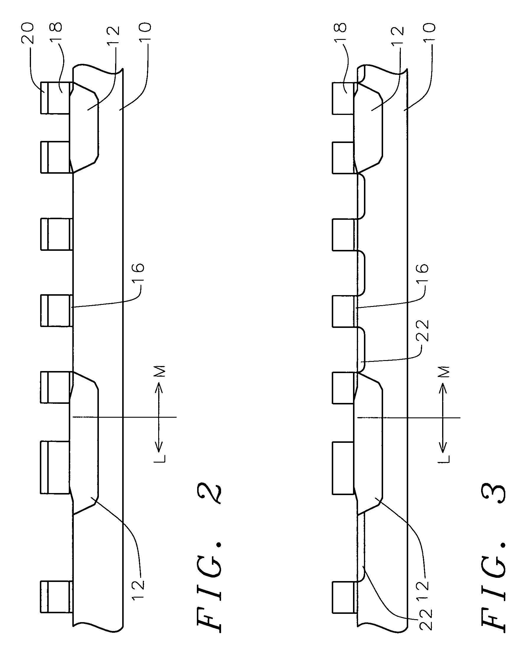
[0018]Referring now more particularly to FIG. 2, there is shown a partially completed integrated circuit device. The semiconductor substrate 10 is preferably composed of silicon having a (100) crystallographic orientation. Semiconductor device structures are formed in and on the semiconductor substrate. For example, isolation regions such as shallow trench isolation (STI) 12 are formed in the semiconductor substrate to separate active areas. A gate oxide layer 16 is grown or deposited on the substrate surface. A polysilicon layer 18 is deposited over the gate oxide layer, followed by a hard mask layer of silicon oxynitride (SiON) 20, for example. The SiON, polysilicon, and gate oxide layers are patterned to form gate electrodes, as shown in FIG. 2, in both the logic area L and the memory area M.

[0019]Now,...


PUM


Abstract

A method for fabricating a metal-insulator-metal capacitor in an embedded DRAM process is described. A plurality of contact plugs are provided through an insulating layer to semiconductor device structures in a substrate wherein the contact plugs are formed in a logic area of the substrate and in a memory area of the substrate and providing node contact plugs to node contact regions within the substrate in the memory area. Thereafter, capacitors are fabricated in a twisted trench in a self-aligned copper process.

Description

[0001]This is a continuation of patent application Ser. No. 10 / 411,347, filing date Apr. 10, 2003, now U.S. Pat. No. 6,720,232, Method Of Fabricating An Embedded DRAM For Metal-Insulator-Metal (MIM) Capacitor Structure, assigned to the same assignee as the present invention, which is herein incorporated by reference in its entirety.BACKGROUND OF THE INVENTION[0002](1) Field of the Invention[0003]The present invention relates to methods of fabricating a metal-insulator-metal capacitor, and more particularly, to methods of forming metal-insulator-metal capacitors for embedded DRAM applications wherein contact etch depth is reduced in the fabrication of an integrated circuit device.[0004](2) Description of the Prior Art[0005]In merging logic circuits and dynamic random access memory (DRAM) arrays on a single chip, compatibility is the primary issue with respect to both design and fabrication. Recently, with the continued decrease in device dimensions, it has become increasingly importa...

Claims


Application Information

Patent Timeline
IPC IPC(8): H01L27/108H01L21/02H01L21/20H01L21/8242
CPCH01L27/10811H01L27/10852H01L27/10894H01L27/10897H01L28/91H10B12/312H10B12/09H10B12/50H10B12/033
Inventor TU, KUO-CHICHEN, CHUN-YAOCHU, HUEY-CHI
Owner TAIWAN SEMICON MFG CO LTD
Why Eureka
Try Eureka