Photonic band gap structure simulator

a technology of gap structure and photon, applied in the field of photon and modeling electronic structures, can solve the problems of not being able to easily determine the appropriate structure or structure for use in a particular situation, not having a convenient system or method, and not being able to perform the necessary calculations in time, so as to achieve the effect of facilitating operation

Inactive Publication Date: 2006-10-03
MASSACHUSETTS INST OF TECH
View PDF16 Cites 5 Cited by
  • Summary
  • Abstract
  • Description
  • Claims
  • Application Information

AI Technical Summary

Benefits of technology

[0007]In one embodiment, a vacuum electron device with a PBG structure can include a PBG structure that is capable of overmoded operation, as well single mode operation. PBG structures are, in some embodiments, two-dimensional (2D) or three-dimensional (3D) periodic structures with restricted transmission bands at certain frequencies. Suc...

Problems solved by technology

Distributed coupling results in relatively small disturbance of the resonant mode frequency when compared with conventional hole coupling.
In the design and construction of suitable PBG cavities, there has not been a convenient system or method for deducing the approp...

Method used


Image

  • Photonic band gap structure simulator
  • Photonic band gap structure simulator
  • Photonic band gap structure simulator

Examples


Embodiment Construction

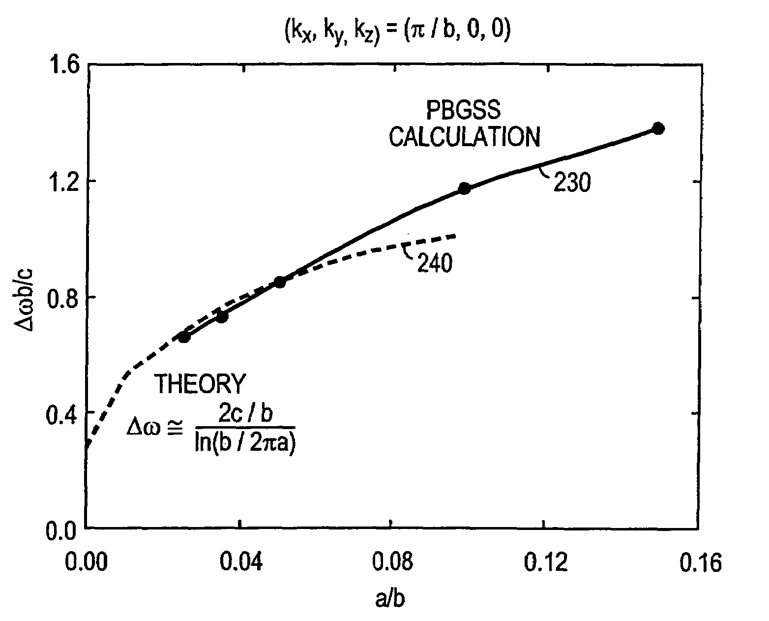
[0040]A brief description of a vacuum electron device having a PBG structure, based on the disclosure in the '661 application, is presented as introductory material to acquaint the reader with the features of PBG structures. The description of the systems and methods used to perform simulations useful in designing and analyzing such PBG structures follows.

[0041]A PBG structure, which is a periodic array of spatially varying dielectric or metallic structures (or combinations of metallic and dielectric structures), was first described by Yablonovitch. In recent years, numerous advances have improved the understanding of the theory of PBG structures. This has led to new applications in passive devices for guiding and confinement of electromagnetic radiation. The use of PBG structures in both microwave and optical devices has primarily been limited to passive devices such as waveguides and filters, though some applications in active devices have been reported.

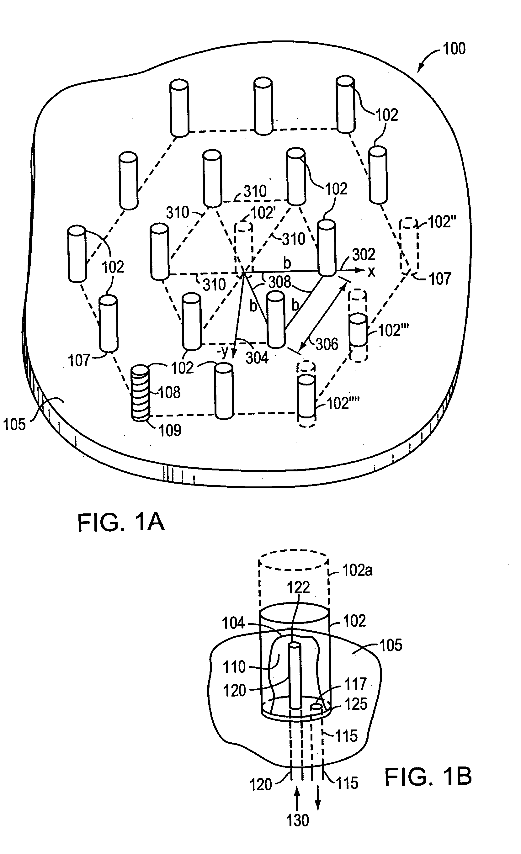
[0042]FIG. 1A is a drawing ...


PUM


Abstract

A system and method for designing photonic band gap structures. The system and method provide a user with the capability to produce a model of a two-dimensional array of conductors corresponding to a unit cell. The model involves a linear equation. Boundary conditions representative of conditions at the boundary of the unit cell are applied to a solution of the Helmholtz equation defined for the unit cell. The linear equation can be approximated by a Hermitian matrix. An eigenvalue of the Helmholtz equation is calculated. One computation approach involves calculating finite differences. The model can include a symmetry element, such as a center of inversion, a rotation axis, and a mirror plane. A graphical user interface is provided for the user's convenience. A display is provided to display to a user the calculated eigenvalue, corresponding to a photonic energy level in the Brilloin zone of the unit cell.

Description

CROSS-REFERENCE TO RELATED APPLICATIONS[0001]This application claims the benefit of U.S. provisional patent application Ser. No. 60 / 298,434, filed Jun. 15, 2001, which application is incorporated herein in its entirety by reference. This application also incorporates by reference the entire disclosure of co-pending U.S. patent application Ser. No. 10 / 037,661, filed Jan. 4, 2002, entitled “Vacuum Electron Device With Photonic Bandgap Structure And Method Of Use Thereof” (hereinafter “the '661 application”), which application is subject to assignment to the same assignee of the present application.GOVERNMENT RIGHTS[0002]This invention was made with government support under Grant No. F49620-99-0197 and Grant No. F49620-01-0007 awarded by the United States Air Force Office of Scientific Research, and Grant No. DE-FG02-95ER40919 awarded by the Department of Energy. The government may have certain rights in the invention.FIELD OF THE INVENTION[0003]This invention relates generally to mode...

Claims


Application Information

Patent Timeline
IPC IPC(8): G06F17/50
CPCG06F17/5018H01P1/2005G06F30/23
Inventor CHEN, CHIPINGSHAPIRO, MICHAEL A.SMIRNOVA, EVGENYA I.TEMKIN, RICHARD J.SIRIGIRI, JAGADISHWAR R.
Owner MASSACHUSETTS INST OF TECH
Why Eureka
Try Eureka