STI formation in semiconductor device including SOI and bulk silicon regions

a technology of semiconductor devices and bulk silicon, which is applied in the direction of semiconductor devices, solid-state devices, transistors, etc., can solve the problems of increasing the demand for integrated circuit customers having more functionality, complex above-described processes, and insufficient isolation in the bulk area, so as to avoid the problem of a subsequent cmp process and reduce complexity

Inactive Publication Date: 2006-10-10
GLOBALFOUNDRIES INC
View PDF8 Cites 233 Cited by
  • Summary
  • Abstract
  • Description
  • Claims
  • Application Information

AI Technical Summary

Benefits of technology

[0008]The invention includes methods for forming or etching silicon trench isolation (STI) in a silicon-on-insulator (SOI) region and a bulk silicon region, and a semiconductor device so formed. The STI can be etched simultaneously in the SOI and bulk silicon regions by etching to an upper-most silicon layer using an STI mask, conducting a timed etch that etches to a desired depth in the bulk silicon region and stops on a buried insulator of the SOI region, and etching through the buried insulator of the SOI region. The buried insulator etch for this process can be done with little complexity as part of a hardmask removal step. Further, by choosing the same depth for both the bulk and SOI regions, problems with a subsequent CMP process are avoided. The invention also cleans up the boundary between the SOI and bulk regions where silicon nitride residuals may exist.

Problems solved by technology

As technologies become increasingly complex, demand for integrated circuits (IC) customer having more functionality is growing.
A challenge that arises relative to providing all of these features is that each feature is optimized under different conditions.
One challenge facing both examples mentioned above is that fabricators must provide isolation of active diffusions for both SOI and bulk regions.
The above-described process is very complicated and cost-ineffective.
In particular, there are a number of challenges with shallow trench isolation (STI) processing relative to patterned SOI versus bulk silicon.
A first challenge relates to the depth of etching for the STI.
A first choice is to use the SOI STI etch depth, which does not give enough isolation in the bulk area.
This process, however, requires an extra photoresist layer and is likely to cause problems with STI planarization.
A second challenge with STI processing in patterned SOI arises from a particular process defect that is intrinsic to wafers created by using the Separation by Implantation of Oxygen (SIMOX) process.
Since polysilicon can be made electrically active either by doping or conversion to silicide divots filled with polysilicon can cause device shorting.
This problem has been observed in early SOI eDRAM hardware.

Method used


Image

  • STI formation in semiconductor device including SOI and bulk silicon regions
  • STI formation in semiconductor device including SOI and bulk silicon regions
  • STI formation in semiconductor device including SOI and bulk silicon regions

Examples


Embodiment Construction

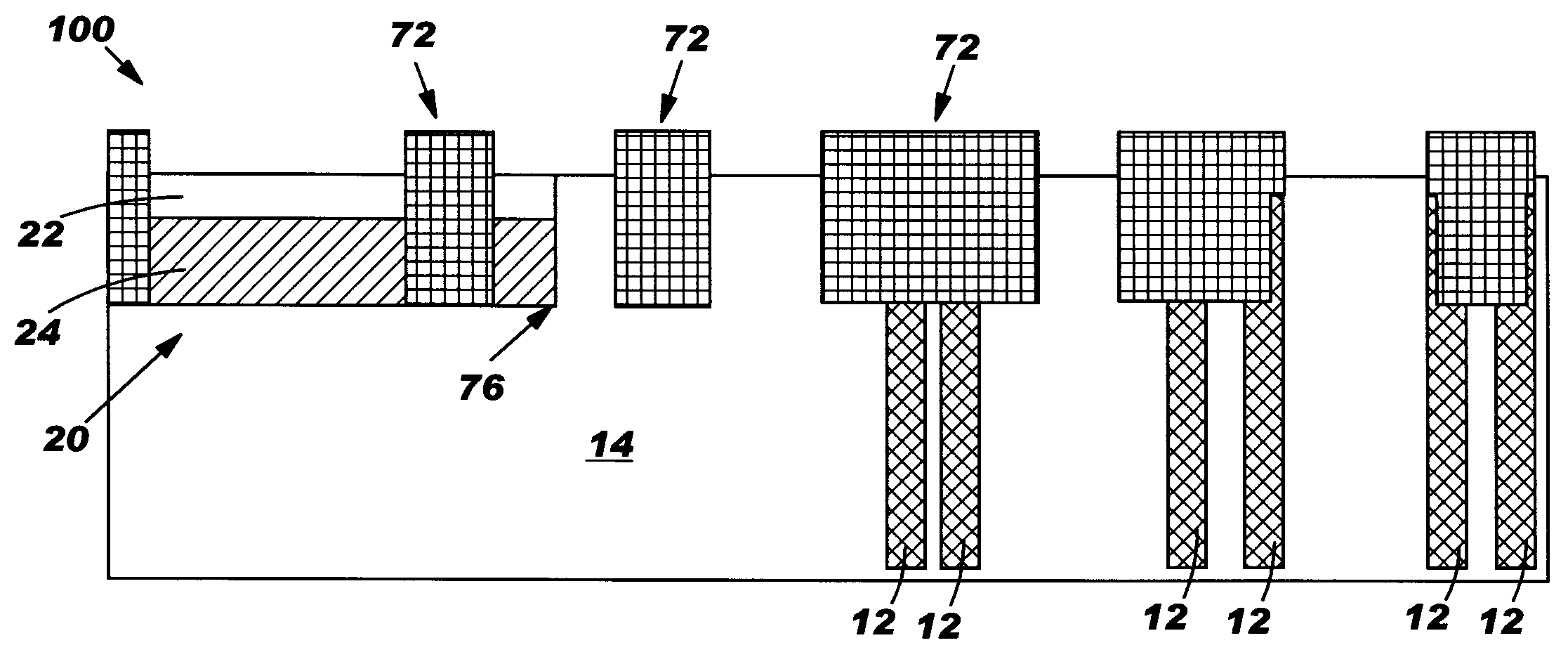
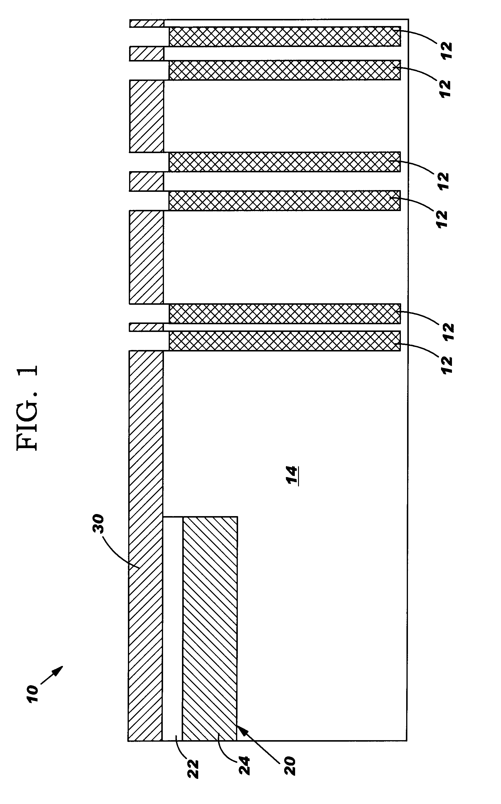
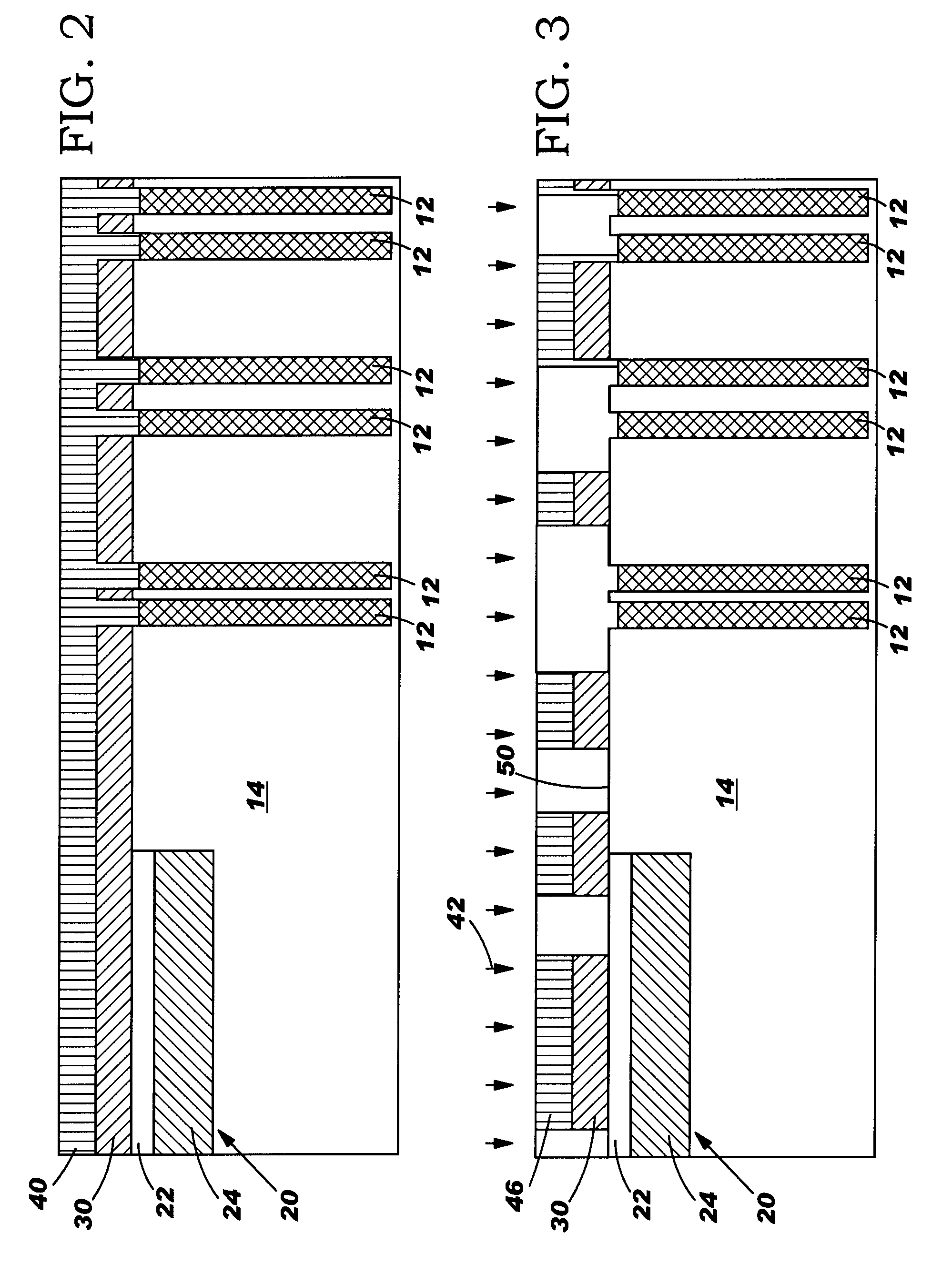
[0018]With reference to the accompanying drawings, FIG. 1 illustrates a cross-sectional view of a typical wafer 10 after deep trench 12 formation in a bulk silicon region 14, and prior to the silicon trench isolation (STI) hardmask deposition. Wafer 10 includes a silicon-on-insulator (SOI) region 20 including a silicon layer 22 on a buried insulator 24. Also included on wafer 10 is a pad layer 30 of, for example, silicon nitride and silicon dioxide.

[0019]In one embodiment, buried insulator 24 material is silicon dioxide, but other materials may also be used. For purpose of illustration only, silicon layer 22 of SOI region 20 may have a thickness of approximately 700A and buried insulator 24 of SOI region 20 may have a thickness of approximately 1350A. Pad layer 30 may have a thickness including approximately 80A of silicon dioxide (not shown due to scale) and approximately 1200A of silicon nitride. It should be recognized, however, that the teachings of the invention are not limited...


PUM

PropertyMeasurementUnit
depthaaaaaaaaaa
thickaaaaaaaaaa
thicknessaaaaaaaaaa

Abstract

Methods for forming or etching silicon trench isolation (STI) in a silicon-on-insulator (SOI) region and a bulk silicon region, and a semiconductor device so formed, are disclosed. The STI can be etched simultaneously in the SOI and bulk silicon regions by etching to an uppermost silicon layer using an STI mask, conducting a timed etch that etches to a desired depth in the bulk silicon region and stops on a buried insulator of the SOI region, and etching through the buried insulator of the SOI region. The buried insulator etch for this process can be done with little complexity as part of a hardmask removal step. Further, by choosing the same depth for both the bulk and SOI regions, problems with a subsequent CMP process are avoided. The invention also cleans up the boundary between the SOI and bulk regions where silicon nitride residuals may exist.

Description

BACKGROUND OF INVENTION[0001]The present invention relates generally to shallow trench isolations (STI), and more particularly, to methods of forming an STI in a semiconductor device including a silicon-on-insulator (SOI) and bulk silicon regions.[0002]As technologies become increasingly complex, demand for integrated circuits (IC) customer having more functionality is growing. In order to provide ICs with optimum designs, high-performance complementary metal-oxide semiconductors (CMOS) devices are required with additional features such as enhanced dynamic random access memory (eDRAM) or radio frequency (RF) applications. A challenge that arises relative to providing all of these features is that each feature is optimized under different conditions. For example, high-performance CMOS may be completed on silicon on insulator (SOI) wafers but RF and eDRAM may be built in bulk silicon.[0003]Conventional techniques exist for making patterned SOI (part bulk and part SOI) wafers for the p...

Claims


Application Information

Patent Timeline
Patent Type & Authority Patents(United States)
IPC IPC(8): H01L21/76H01L21/308H01L21/311H01L21/316H01L21/762
CPCH01L21/3081H01L21/76283H01L21/31612H01L21/7624
Inventor STEIGERWALT, MICHAEL D.KUMAR, MAHENDERHO, HERBERT L.DOBUZINSKY, DAVID M.FALTERMEIER, JOHNATHAN E.PENDLETON, DENISE
Owner GLOBALFOUNDRIES INC
Why Eureka
Try Eureka