
Wafer thinning using magnetic mirror plasma

a technology of magnetic mirror plasma and wafer thinning, which is applied in the direction of vacuum evaporation coating, electrolysis components, coatings, etc., can solve the problems of non-use of magnetic mirror fields and substrate processing, and achieve low variance thickness and optimize dissociation of complex process gases

Inactive Publication Date: 2006-10-10
IFIRE TECH INC
View PDF6 Cites 6 Cited by
  • Summary
  • Abstract
  • Description
  • Claims
  • Application Information

AI Technical Summary

Benefits of technology

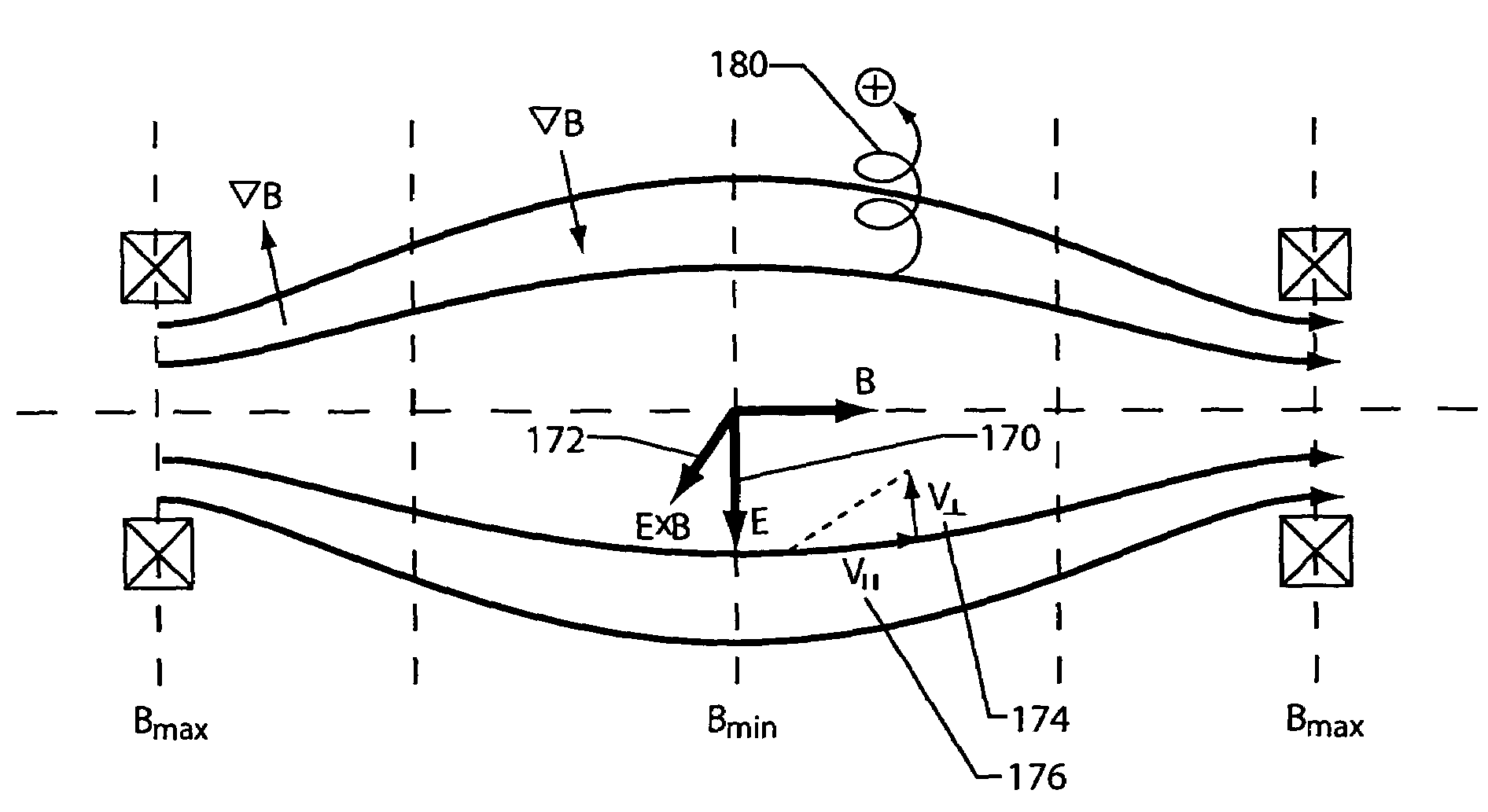
"The invention is a system for thinning wafers using a magnetic mirror plasma etcher. The system may include additional etchers such as dry etchers, wet etchers, or a combination of both. The magnetic mirror plasma uses a unique method to confine a plasma using a magnetic mirror field and an orthogonally rotating electric field. The system may also include a chamber constructed of non-ferrous material to house the substrate being processed. The invention also includes methods for segregating IC chips within a wafer and exposing vias on the backside of an IC chip. The technical effects of the invention include improved plasma confinement, reduced substrate damage, and improved process control."

Problems solved by technology

Magnetic mirror fields have typically not been used in the most common plasma process application of semiconductor thin film etch and deposition due to substrate damage.
In the case of high energy physics and fusion energy experimentation, substrate processing is not the objective.
Rather, plasma confinement is the primary objective of these high energy experiments and as such orthogonal electric fields have been considered to be a detriment.

Method used


Image

  • Wafer thinning using magnetic mirror plasma
  • Wafer thinning using magnetic mirror plasma
  • Wafer thinning using magnetic mirror plasma

Examples


Embodiment Construction

[0038]WLP and flip chip with bump designs are useful for applications where higher functionality per unit volume is required and not available with conventional packaging approaches. These include, but are not limited to, portable, battery powered devices like cell phones, personal digital assistants, notebook computers, camcorders, and smart cards, among others. Moreover, functional and performance improvements such as stacked die, better temperature survivability and faster performance (due to reduced parasitic capacitance) may be achieved with thinner wafers.

[0039]In wafer level processing (WLP), processing steps such as final test, burn-in, and memory array repair may be performed prior to segregation. Economies improve with larger wafers. However, larger wafers typically have greater thickness to prevent breakage during front side processing. Typical wafer thinning techniques are limited in the thickness they may achieve.

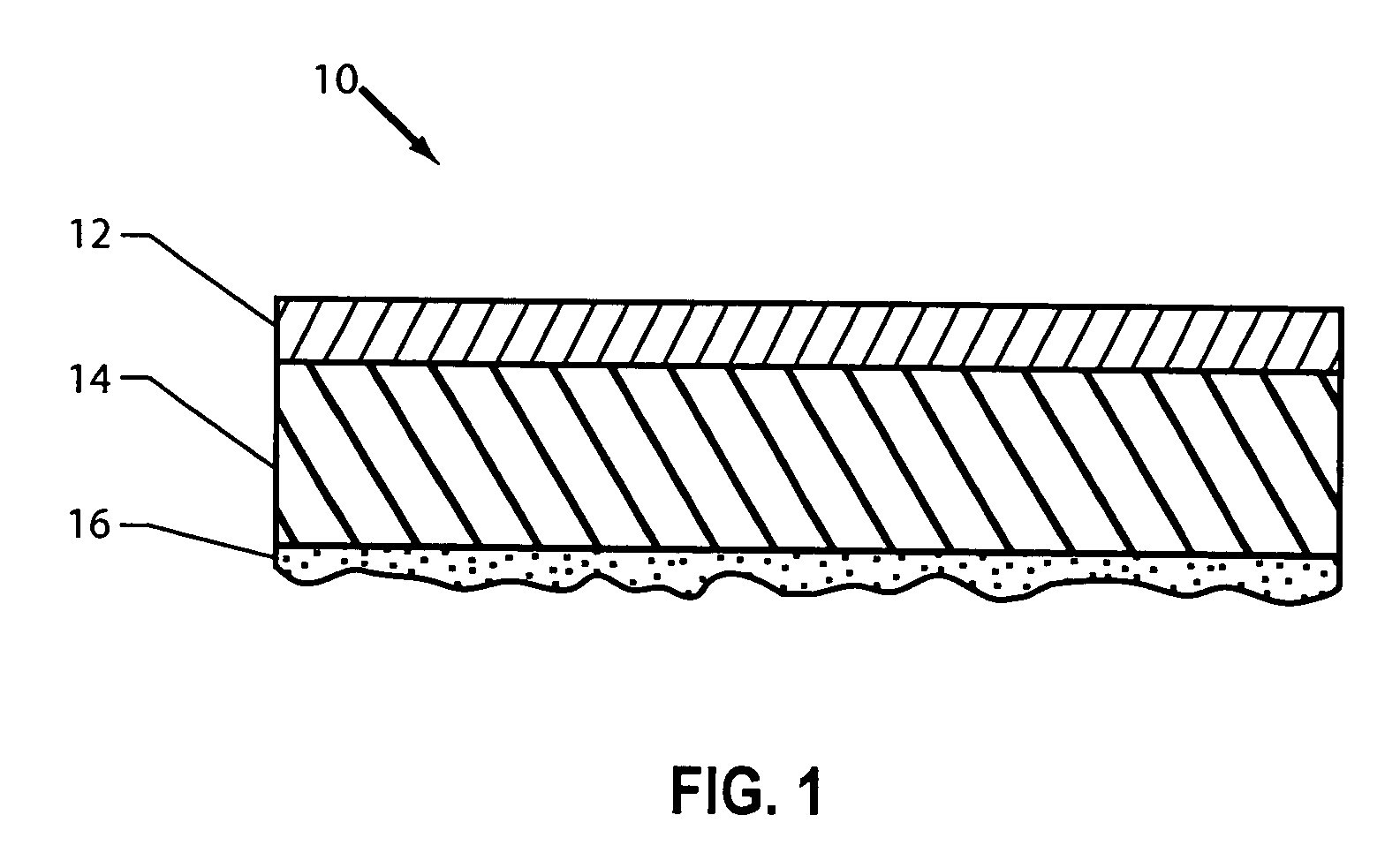
[0040]FIG. 1 is a cross section illustration of an exempl...


PUM

PropertyMeasurementUnit
thickaaaaaaaaaa
diameteraaaaaaaaaa
diameteraaaaaaaaaa

Abstract

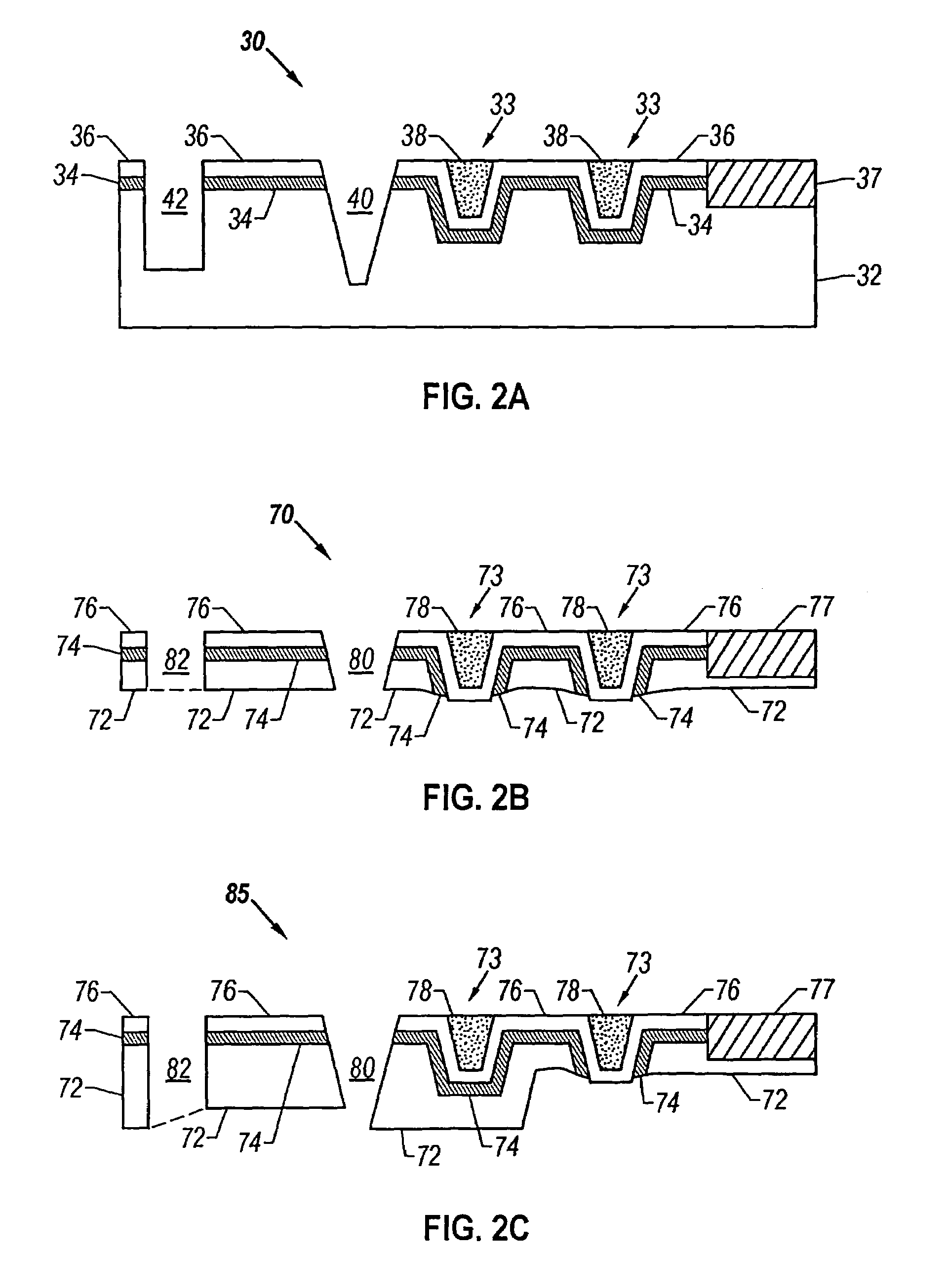
A method for manufacturing integrated circuits uses an atmospheric magnetic mirror plasma etching apparatus to thin a semiconductor wafer. In addition the process may, while thinning, both segregate and expose through-die vias for an integrated circuit chip. To segregate, the wafer may be partially diced. Then, the wafer may be tape laminated. Next, the backside of the wafer may be etched. As the backside material is removed, the partial dicing and through-die vias may be exposed. As such, the method reduced handling steps and increases yield. Furthermore, the method may be used in association with wafer level processing and flip chip with bump manufacturing.

Description

RELATED APPLICATIONS[0001]This application is a continuation-in-part of U.S. patent application Ser. No. 10 / 390,977, filed , which is now U.S. Pat. No. 6,794,272, issued on Sep. 21, 2004, which is a continuation-in-part of U.S. patent application Ser. No. 10 / 133,296, filed Apr. 26, 2002, which claims priority of U.S. patent Application Ser. No. 60 / 336,786, filed Oct. 26, 2001, entitled: “Wafer Thinning Process”, and is incorporated by reference in its entirety hereinTECHNICAL FIELD OF THE INVENTION[0002]This invention relates in general to a system and method for integrated circuit manufacturing. More specifically, this application relates to a system and method for thinning integrated circuit wafers which include using a magnetic mirror plasma process.BACKGROUND OF THE INVENTION[0003]The increasing demand for portable products is driving semiconductor device design to place a premium on package size and density (smaller, thinner, cheaper, and with higher functionality per unit volu...

Claims


Application Information

Patent Timeline
Patent Type & Authority Patents(United States)
IPC IPC(8): H01L21/461H01L21/78H01L21/301H01L21/304H01L21/768H01L23/48
CPCH01L21/76898H01L21/78H01L23/481H01L21/304Y10S438/977H01L2924/0002H01L2924/00012H01L2924/00H01L21/3065
Inventor TURNER, TERRY R.SPAIN, JAMES D.BANKS, RICHARD M.
Owner IFIRE TECH INC
Learn More