Isoelectronic surfactant suppression of threading dislocations in metamorphic epitaxial layers

a technology of epitaxial layer and isoelectronic surfactant, applied in the field of isoelectronic surfactant suppression of threading dislocation in metamorphic epitaxial layer, can solve the problems of optoelectronic device cost, similar dilemma, etc., and achieve the effect of reducing the propagation of threading dislocations

Active Publication Date: 2006-10-17
THE BOEING CO
View PDF22 Cites 84 Cited by
  • Summary
  • Abstract
  • Description
  • Claims
  • Application Information

AI Technical Summary

Benefits of technology

[0025]In one aspect of the invention, a method of reducing propagation of threading dislocations into active areas of a III–V optoelectronic device includes growing a plurality o

Problems solved by technology

A basic problem is that devices are optimal for applications in regions of band gap where there is no available substrate.
A similar dilemma continues to most optoelectronic devices—such as lasers, LEDs, HBTs, and others—where the most suitable band gaps are not the ones easily available near a lattice constant of an available substrate.
Another restriction this imposes is in the cost of the available substrates for a given device.
For example, InP is available, but is very costly and may make certain optoelectronic designs too expensive to be commercially practical.
But the thickness of these layers that can be grown before plastic deformation occurs is typically limited.
The device designs are limited to layers where no relaxation or limited relaxation has occurred and thus limited to certain amounts of strain and thickness.
The number or density of loops is a kinetic or rate problem.
The presence of threading dislocations in the active regions of a device may act as a loss mechanism, degrading the performance of the device.
This thickness requirement restricts the usefulness of intentionally engineering the strain within a given device to near atomic layer dimensions for large strains.
One may attack the problem of strained, mismatched active device layers by controlling the growth conditions and composition to keep the designed layers below the strain and thickness parameters.
As stated above, this limits the available alloys and thicknesses for device designs and may be highly disadvantageous for device performance.
The other extreme in this problem is to intentionally form 100% relaxed layers, but confine the relaxation to inactive regions of the device.
The drawback to this method is that forcing the relaxation to occur typically leads to large densities of threading

Method used


Image

  • Isoelectronic surfactant suppression of threading dislocations in metamorphic epitaxial layers
  • Isoelectronic surfactant suppression of threading dislocations in metamorphic epitaxial layers
  • Isoelectronic surfactant suppression of threading dislocations in metamorphic epitaxial layers

Examples


examples

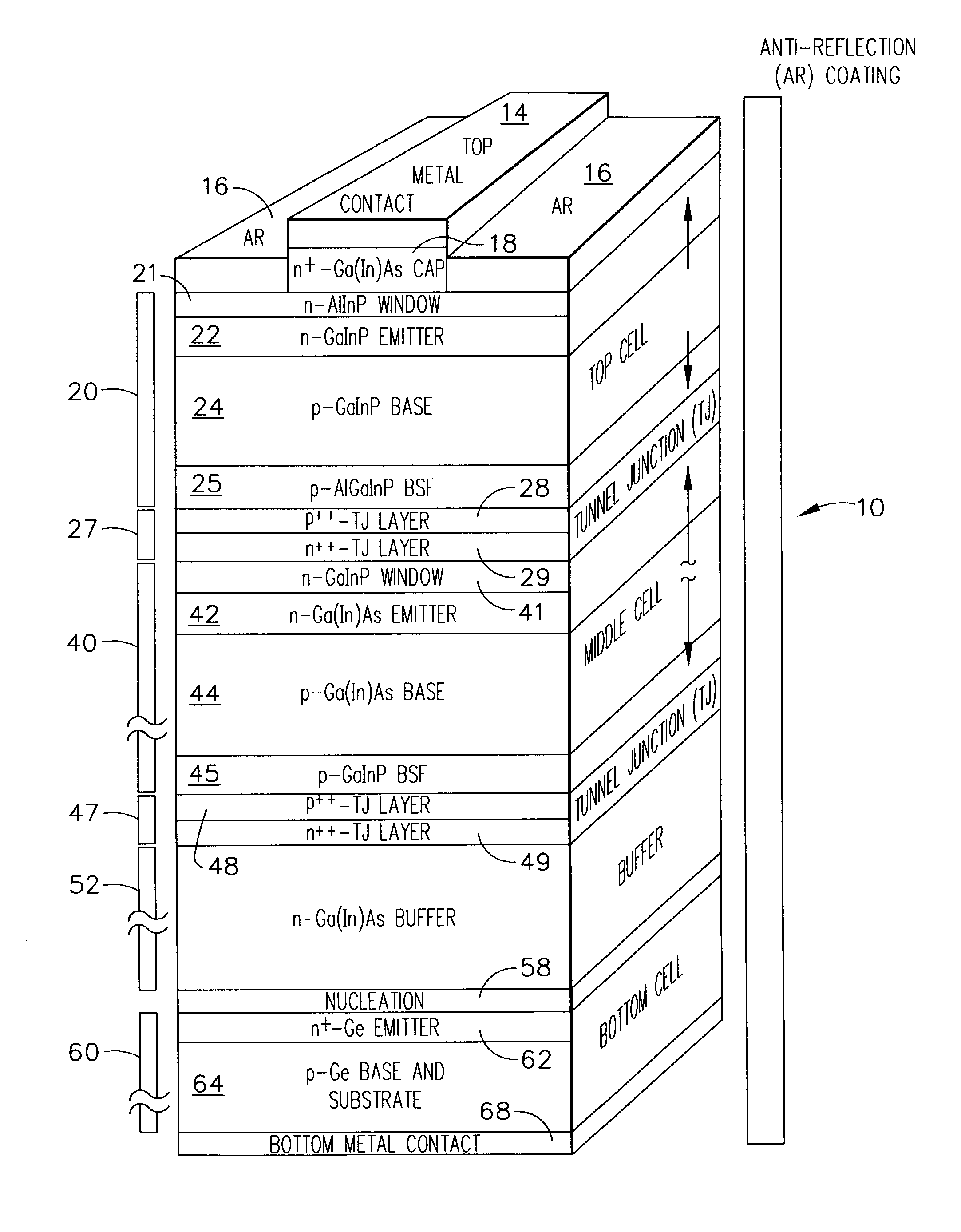
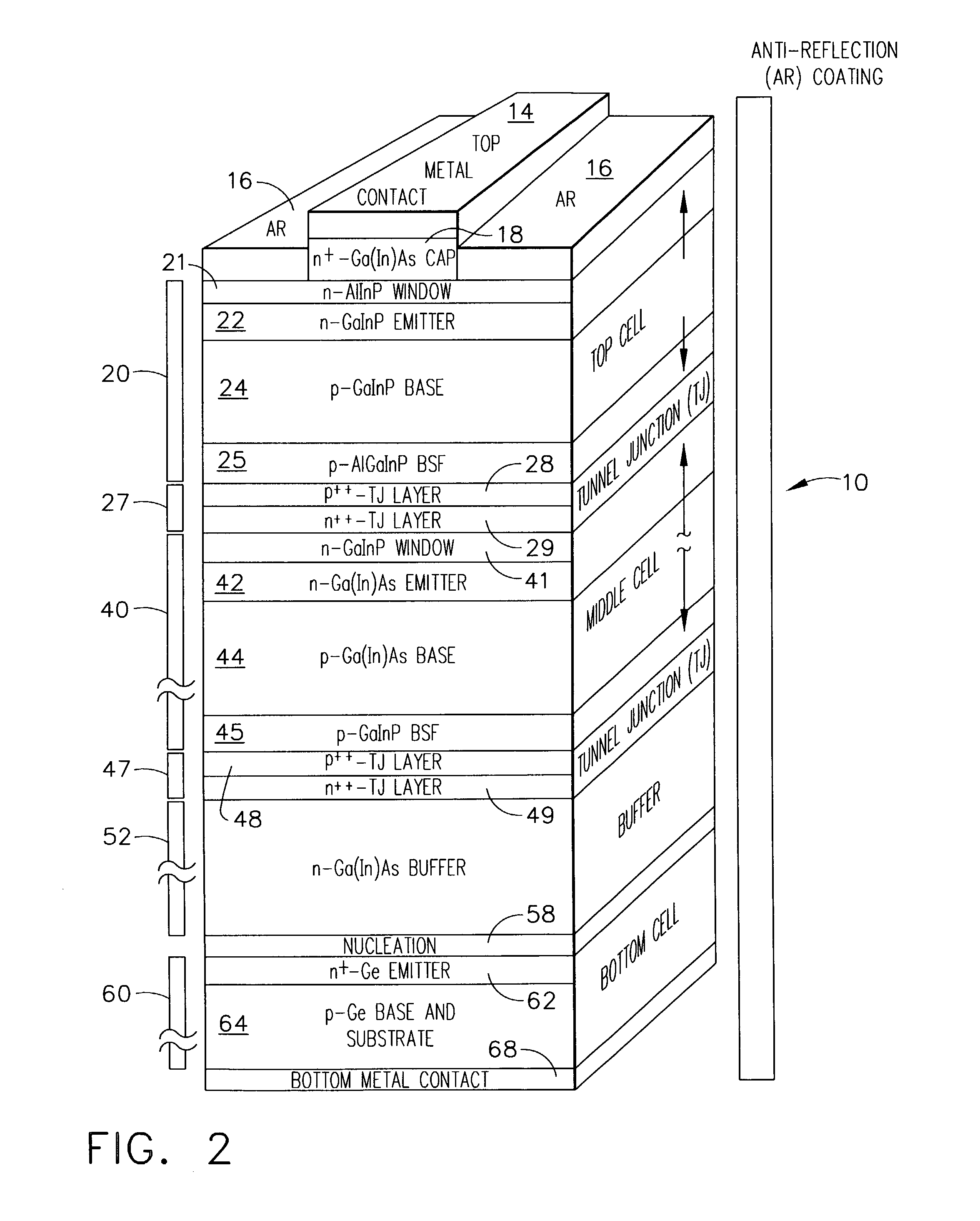
[0082]Monolithic 2-junction metamorphic GaInP / GaInAs / Ge solar cells with a middle cell 40 indium content of 12% In and the middle-cell-active-only (isocells) were fabricated and tested as described below.

[0083]Using the structure depicted in FIG. 2, non-anti-reflective coated 1 cm×1 cm cells were fabricated and tested for the condition of Sb in the buffer layer 52 as compared to samples grown without Sb the buffer layer 52. The cells fabricated were in a dual-junction configuration with the top cell electrically deactivated for both conditions by growing the top cell layers with the same doping type (isotype top cell layers). The measured open-circuit voltage (Voc) voltage at maximum power (Vmp), fill factor (FF) and efficiency are shown in FIGS. 6a–c. Error bars shown are plus and minus one times the standard deviation for the entire cell population tested.

[0084]The addition of Sb to the buffer layer 52 resulted in an increase of approximately 100 mV in Voc as compared to the contr...


PUM


Abstract

A method of reducing propagation of threading dislocations into active areas of an optoelectronic device having a III–V material system includes growing a metamorphic buffer region in the presence of an isoelectronic surfactant. A first buffer layer may be lattice matched to an adjacent substrate and a second buffer layer may be lattice matched to device layers disposed upon the second buffer layer. Moreover, multiple metamorphic buffer layers fabricated in this manner may be used in a single given device allowing multiple layers to have their band gaps and lattice constants independently selected from those of the rest of the device.

Description

GOVERNMENT RIGHTS[0001]This invention was made with Government support under contract no. F29601-98-2-0207 awarded by the U.S. Air Force. The government has certain rights in this invention.BACKGROUND OF THE INVENTION[0002]The present invention generally relates to semiconductor materials and to a method of reducing the propagation of threading dislocations from plastic deformation in mismatched epitaxial layers into active areas of optoelectronic devices and, more particularly, to a method for reducing the propagation of such dislocations for solar energy conversion and other photovoltaic devices.[0003]The interest in photovoltaic (PV) cells in both terrestrial and non-terrestrial applications continues as concerns over pollution and limited resources increases. Irrespective of the application, and as with any energy generation system, efforts have been ongoing to increase the output and / or increase the efficiency of PV cells. To increase the electrical power output of such cells, ...

Claims


Application Information

Patent Timeline
IPC IPC(8): H01L31/04H01L31/18H01L21/20H01L21/205H01L21/365H01L31/00
CPCH01L31/184H01L21/02381H01L21/02439H01L21/0245H01L21/02463H01L21/02505H01L21/02543Y02E10/544
Inventor FETZER, CHRISTOPHER M.ERMER, JAMES H.KING, RICHARD R.COTLER, PETER C.
Owner THE BOEING CO
Why Eureka
Try Eureka