Semiconductor device with perovskite capacitor

a technology of perovskite and capacitor, which is applied in the direction of capacitors, solid-state devices, transistors, etc., can solve the problems of difficult to form conductive perovskite type metal oxide films having preferable crystallinity, difficult to form dielectric films, and difficult to form pzt films of good crystallinity, etc., to achieve the effect of reducing gibbs free energy

Inactive Publication Date: 2006-10-17
KK TOSHIBA
View PDF6 Cites 9 Cited by
  • Summary
  • Abstract
  • Description
  • Claims
  • Application Information

AI Technical Summary

Problems solved by technology

However, it is not easy to form a PZT film of good crystallinity and orientation on the SRO film formed on the Pt film.
The foregoing problem generally occurs in the combination of conductive perovskite type metal oxide film and noble metal film (or noble metal oxide film) in addition to the combination of SRO film and PT film.
In this case, it is difficult to form the conductive perovskite type metal oxide film having preferable crystallinity.
Thus, it is difficult to form a dielectric film, such as PZT film, excellent in crystallinity.
As a result, there is the problem of remarkably reducing capacitor characteristics and reliability.

Method used


Image

  • Semiconductor device with perovskite capacitor
  • Semiconductor device with perovskite capacitor
  • Semiconductor device with perovskite capacitor

Examples


first embodiment

[0027](First Embodiment)

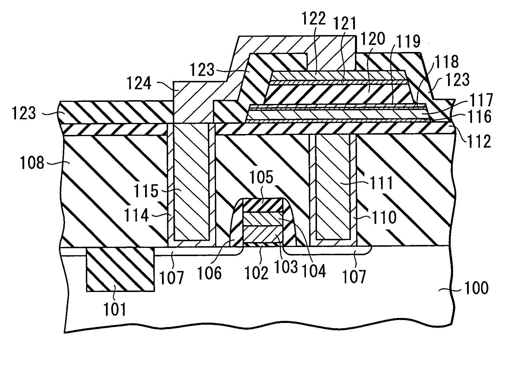
[0028]FIG. 1A to FIG. 1C are cross-sectional views showing the process of manufacturing a semiconductor device according to a first embodiment of the present invention.

[0029]As shown in FIG. 1A, an isolation region 101 having STI (Shallow Trench Isolation) structure is formed on a p-type silicon substrate (semiconductor substrate) 100. A MIS transistor is formed in the following manner.

[0030]A silicon oxide film having a thickness of about 6 nm is formed as a gate insulating film 102 by thermal oxidation. An n+-type polysilicon film 103 doped with arsenic is formed on the gate insulating film 102. A WSix film 104 and a silicon nitride film 105 are further formed on the polysilicon film 103. Thereafter, polysilicon film 103, WSix film 104 and silicon nitride film 105 are processed by normal photolithography and RIE so that a gate electrode can be formed. A silicon nitride film 106 is deposited on the entire surface. An RIE is carried out so that a sidewall spa...

second embodiment

[0056](Second Embodiment)

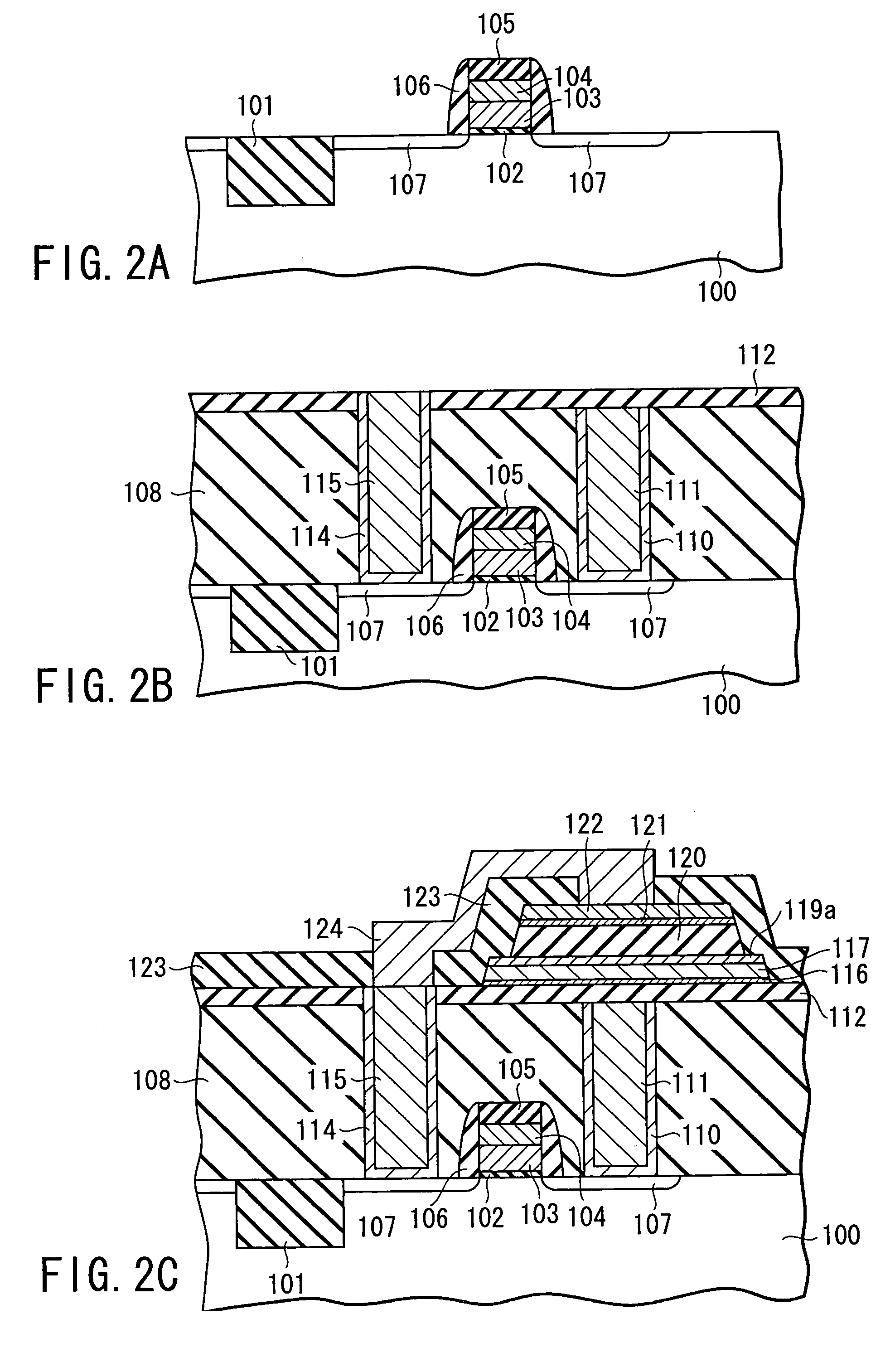
[0057]FIG. 2A to FIG. 2C are cross-sectional views showing the process of manufacturing a semiconductor device according to a second embodiment of the present invention.

[0058]The processes of FIG. 2A and FIG. 2B are substantially the same as FIG. 1A and FIG. 1B of the first embodiment; therefore, the explanation is omitted.

[0059]After the process of FIG. 2B, as shown in FIG. 2C, the following films are successively deposited by sputtering. That is, a titanium film 116 having a thickness of 10 nm is formed, and a platinum film 117 having a thickness of 100 nm is formed as a noble metal film. Further, an SRO film (Sr(Ru,Ti)O3 film) 119a doped with titanium having a thickness of 3 nm is formed as a conductive perovskite type metal oxide film by sputtering. RTA (Rapid Thermal Annealing) is carried out in oxygen atmosphere, and thereby, the SRO film 119a doped with titanium is crystallized. In this case, the SRO film 119a is deposited at the temperature of 550° C...

third embodiment

[0065](Third Embodiment)

[0066]FIG. 3A to FIG. 3C are cross-sectional views showing the process of manufacturing a semiconductor device according to a third embodiment of the present invention.

[0067]The processes of FIG. 3A and FIG. 3B are substantially the same as FIG. 1A and FIG. 1B of the first embodiment; therefore, the explanation is omitted.

[0068]After the process of FIG. 3B, as shown in FIG. 3C, the following films are successively deposited by sputtering. That is, a titanium film 116 having a thickness of 10 nm is formed, and iridium film 117a having a thickness of 100 nm is formed as a noble metal film. Further, a platinum film 117b having a thickness of 50 nm is formed as a noble metal film, and a titanium film 118 having a thickness of 2 nm is formed as a metal film. Further, an SrRuO3 film (SRO film) 119 having a thickness of 3 nm is formed as a conductive perovskite type metal oxide film. RTA (Rapid Thermal Annealing) is carried out in oxygen atmosphere, and thereby, the...


PUM

PropertyMeasurementUnit
thicknessaaaaaaaaaa
thicknessaaaaaaaaaa
surface roughnessaaaaaaaaaa

Abstract

A semiconductor device comprising a semiconductor substrate, and a capacitor provided above the semiconductor substrate, and including a bottom electrode, a top electrode and a dielectric film between the bottom and top electrodes, the bottom electrode including a conductive film selected from a noble metal film and a noble metal oxide film, a metal oxide film having a perovskite structure, provided between the dielectric film and the conductive film, expressed by ABO3, and containing first metal element as B-site element, and a metal film provided between the conductive film and the metal oxide film, and containing second metal element which is B-site element of a metal oxide having a perovskite structure, a decrease of Gibbs free energy when the second metal element forms oxide being larger than that when the first metal element forms oxide, a thickness of the metal oxide film being 5 nm or less.

Description

CROSS-REFERENCE TO RELATED APPLICATIONS[0001]This application is based upon and claims the benefit of priority from prior Japanese Patent Application No. 2003-129072, filed May 7, 2003, the entire contents of which are incorporated herein by reference.BACKGROUND OF THE INVENTION[0002]1. Field of the Invention[0003]The present invention relates to a semiconductor device. In particular, the present invention relates to a semiconductor device having a capacitor.[0004]2. Description of the Related Art[0005]Recently, there have been advanced the research and development of ferroelectric memory (FeRAM: Ferroelectric Random Access Memory) using ferroelectric film as a capacitor dielectric film.[0006]A Pb(ZrXTi1-X)O3 film (PZT film) or an SrBi2Ta2O9 film (SBT film) is given as a typical ferroelectric film used for the ferroelectric memory. PZT is a perovskite compound, and the SBT is a Bi aurivillius phase compound having a pseudo perovskite structure.[0007]If a PZT film is used as the ferr...

Claims


Application Information

Patent Timeline
Patent Type & Authority Patents(United States)
IPC IPC(8): H01L29/76H01L29/94H01L31/062H01L31/113H01L31/119H01L21/316H01L21/02H01L21/8246H01L27/105H01L27/108H01L27/115H01L27/11507
CPCH01L27/11502H01L27/11507H01L28/65H01L28/55H10B53/30H10B53/00
Inventor ITOKAWA, HIROSHIYAMAKAWA, KOJINATORI, KATSUAKI
Owner KK TOSHIBA
Why Eureka
Try Eureka