Optical control element

a control element and optical control technology, applied in the field can solve the problems of preventing high-speed communication, large size of optical control elements, low degree of freedom in dispersion properties, etc., and achieve the effects of small size, low loss, and small siz

Active Publication Date: 2006-10-17
RICOH KK +1
View PDF11 Cites 24 Cited by
  • Summary
  • Abstract
  • Description
  • Claims
  • Application Information

AI Technical Summary

Benefits of technology

[0020]A first specific object of the present invention is to provide an optical control element having a small size and low loss and capable of group speed control of short light pulses.
[0021]A second specific object of the present invention is to provide an optical control element having a small size and low loss, and having a large dispersion control effect and a large group speed delay effect.
[0022]A third specific object of the present invention is to provide an optical control element having a small size and low loss, and having a large dispersion control effect and a large group speed delay effect, while enabling easy control of a refraction index of a constituent material and enabling easy fabrication.
[0023]A fourth specific object of the present invention is to provide an optical control element capable of dispersion control and group speed delay control in a wide frequency region with high precision.
[0049]According to the present invention, it is possible to provide an optical control element that can be made small and has a low loss, and is capable of group speed control and wavelength dispersion control with short pulsed light.

Problems solved by technology

This problem prevents high speed communication.
However, in the above device, a long optical fiber has to be used; for this reason, the optical control element becomes large in size, and has a low degree of freedom in the dispersion property.
Due to this, it is difficult to reduce the size of the optical control device and increase the degree of integration, which are required for high level signal processing or multiple lines parallel processing.
However, in order to achieve dispersion compensation, an optical fiber of an order of meters has to be used, hence it is difficult to reduce the size of the optical control device and increase the degree of integration.
Further, because in a device including the chirped structure fiber grating, the incident light has to be reflected for use, and a circulator is needed to obtain high efficiency, hence, it is difficult to reduce the size of the optical control device and increase the degree of integration.
However, in the dispersion compensation devices disclosed in reference 1 and reference 2, because the light propagating in the photonic crystal is not confined inside the wave guide structure, the dispersion compensation devices exhibit strong angular dependence, and have problems in reliability.
Further, it is difficult to reduce the size of the dispersion compensation devices.
For these reasons, these dispersion compensation devices disclosed in reference 1 and reference 2 cannot be put into practical use.
For this reason, it is difficult to obtain a device for dispersion control and group speed control by using such a simple defect wave guide.
However, in a slab type photonic crystal, which has been studied long before and is easy to be fabricated, if the coupled defect wave guide is formed, the period of the coupled defect wave guide in the propagation direction of the light is long, hence it is difficult to avoid a light leakage condition, known as “light-cone”, consequently, a large loss of light occurs.
Due to this, the photonic crystal cannot be put into practical use at all.
However, in this method, the light propagates in the space but not in a wave guide, so it is difficult to reduce the size of the device and increase the degree of integration.

Method used


Image

  • Optical control element
  • Optical control element
  • Optical control element

Examples


first embodiment

[0093

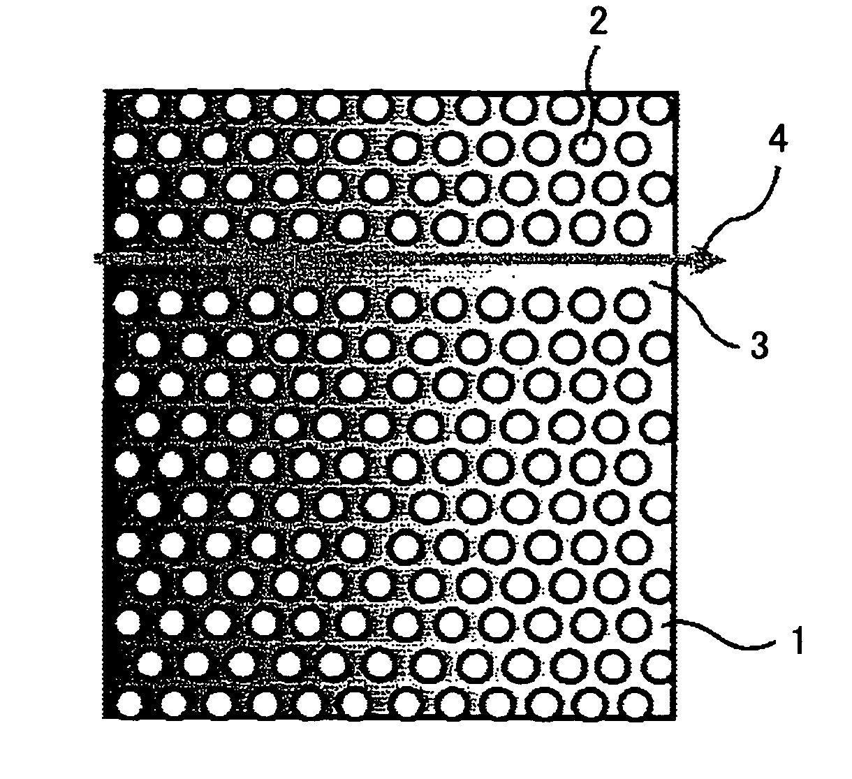
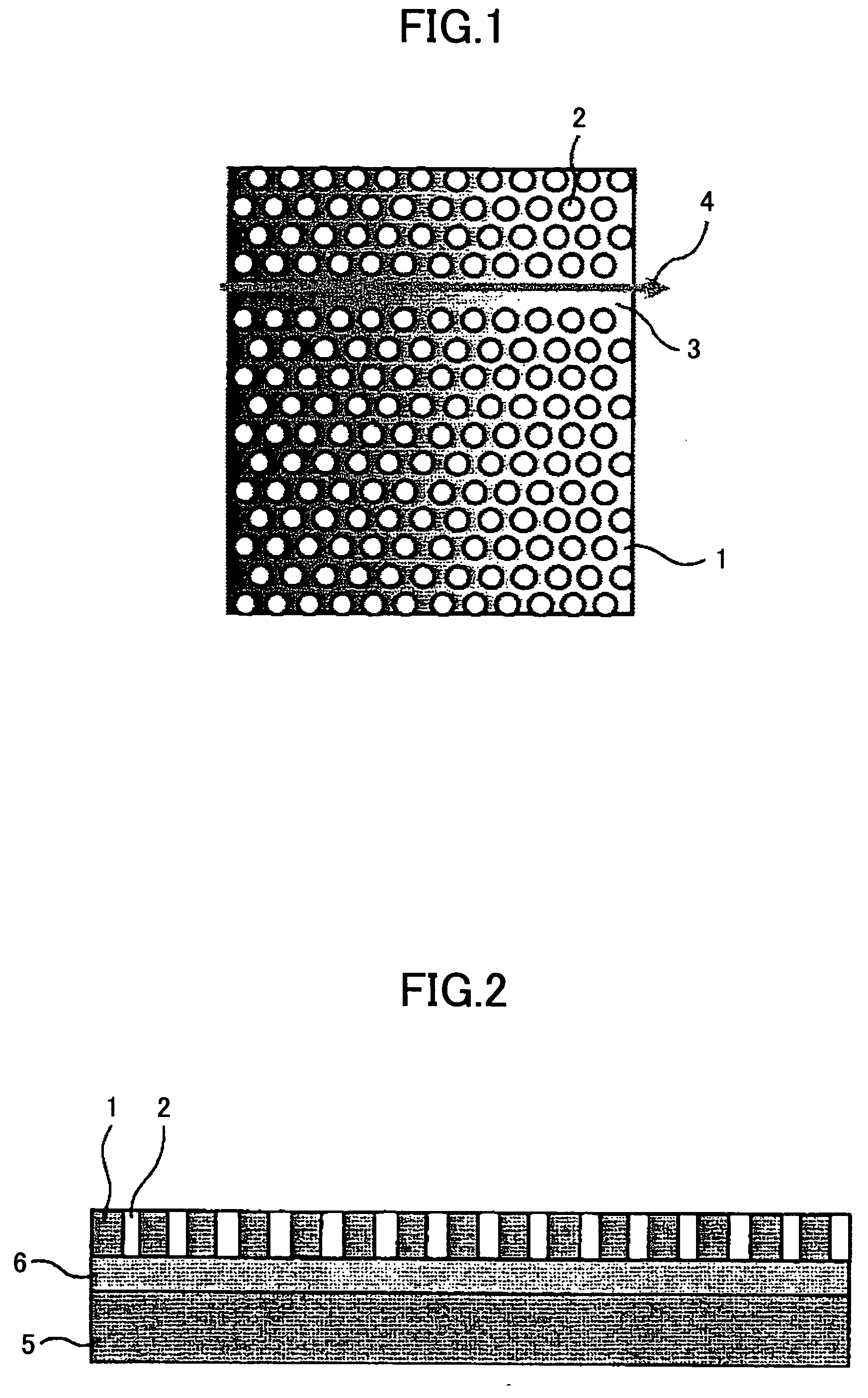
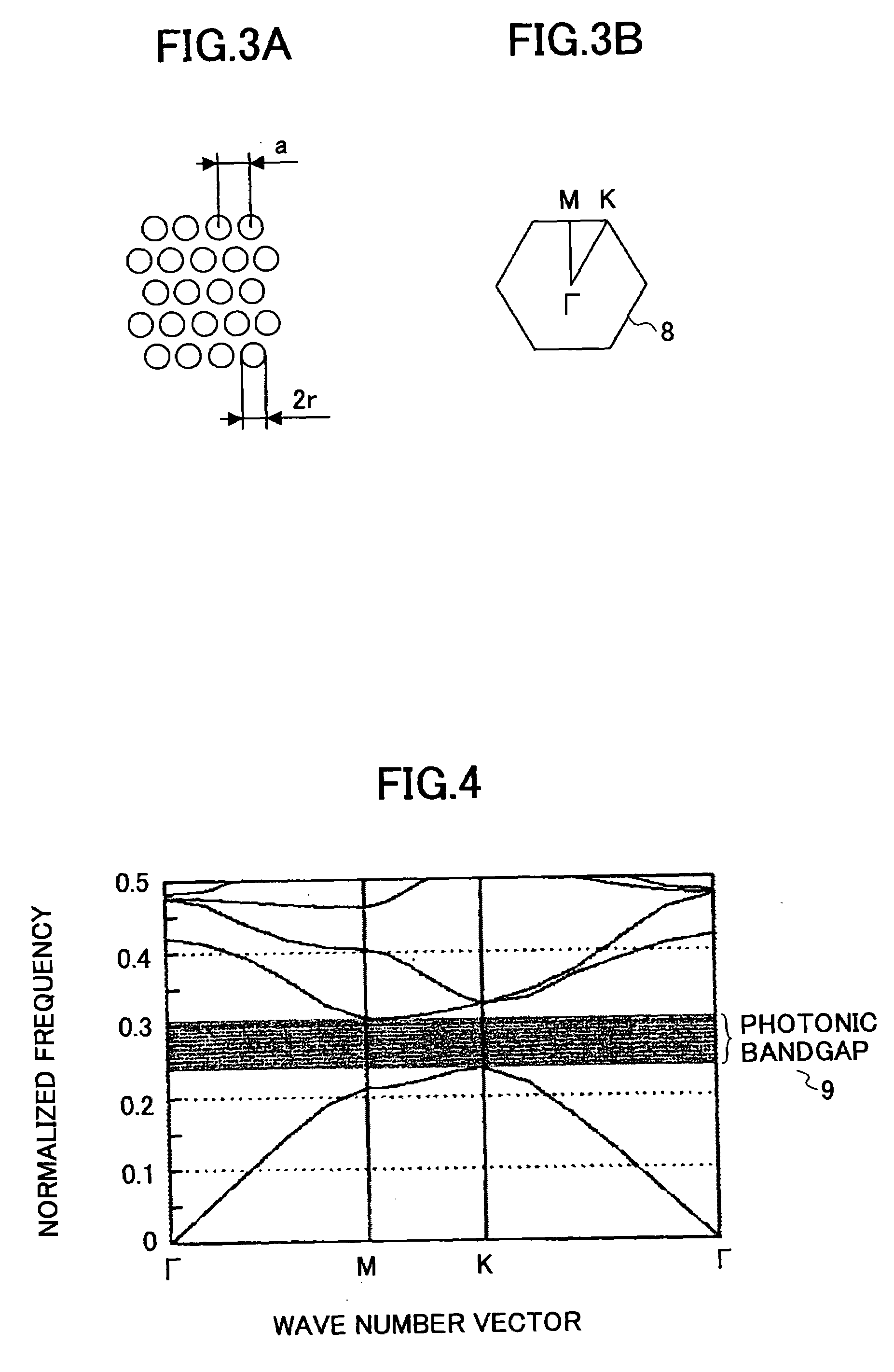
[0094]FIG. 1 is a schematic view of an optical control element formed from a slab type two-dimensional photonic crystal according to a first embodiment of the present invention.

[0095]The optical control element shown in FIG. 1 includes a thin film 1 having a distributed refraction index, photonic crystal holes 2, and a defect wave guide 3. As shown in FIG. 1, light 4 is guided by the defect wave guide 3. In FIG. 1, the photonic crystal includes the thin film 1 formed from a material having a high refraction index and holes 2 formed from a material having a low refraction index. In addition, in FIG. 1, the left portion of the thin film 1 has a relatively high refraction index, and the right portion of the thin film 1 has a relatively low refraction index. The refraction index of the thin film 1 is arranged so that the refraction index of the material of the thin film 1 and the holes 2, or the difference of the effective refraction indexes between the thin film 1 and the holes 2,...

second embodiment

[0131

[0132]Below, the second embodiment of the present invention is explained with reference to FIG. 6 and FIGS. 7A and 7B. In the present embodiment, the same reference numbers are used for the same elements as those in the previous embodiment.

[0133]FIG. 6 is a schematic view of an optical control element formed from a slab type two-dimensional photonic crystal according to the second embodiment of the present invention.

[0134]The optical control element shown in FIG. 6 includes a thin film 10 having a distributed refraction index, photonic crystal holes 2, and a defect wave guide 3. As shown in FIG. 6, light 4 is guided by the defect wave guide 3. In FIG. 6, the photonic crystal includes the thin film 10 formed from a material having a high refraction index and holes 2 formed from a material having a low refraction index. Furthermore, in FIG. 6, the left portion of the thin film 10 has a relatively high refraction index, and the right portion of the thin film 10 has a relatively lo...

third embodiment

[0145

[0146]Below, the third embodiment of the present invention is explained with reference to FIG. 8. In the present embodiment, the same reference numbers are used for the same elements as those in the previous embodiments.

[0147]FIG. 8 is a schematic view of an optical control element formed from a slab type two-dimensional photonic crystal according to the third embodiment of the present invention.

[0148]The optical control element shown in FIG. 8 includes a thin film 10 having a distributed refraction index, photonic crystal holes 2, and a defect wave guide 3. As shown in FIG. 8, light 4 is being guided by the defect wave guide 3. In FIG. 8, the photonic crystal includes the thin film 10 formed from a material having a high refraction index and holes 2 formed from a material having a low refraction index. Furthermore, in FIG. 8, the left portion of the thin film 10 has a relatively high refraction index, and the right portion of the thin film 10 has a relatively low refraction in...


PUM

PropertyMeasurementUnit
diameteraaaaaaaaaa
diameteraaaaaaaaaa
diameteraaaaaaaaaa

Abstract

An optical control element is disclosed that can be made small and has a low loss, and is able to provide group speed control and wavelength dispersion of short light pulses. The optical control element is formed from a photonic crystal, and includes a first portion having a first refraction index in the photonic crystal, a second portion having a second refraction index lower than the first refraction index, and a refraction-index-distributed type defect wave guide. A difference effective refraction indexes between the first portion and the second portion near the refraction-index-distributed type defect wave guide, changing continuously or stepwise along a wave guiding direction of the refraction-index-distributed type defect wave guide.

Description

BACKGROUND OF THE INVENTION[0001]1. Field of the Invention[0002]The present invention relates to an optical control element using a photonic crystal, and more particularly, relates to an optical control element that is able to be made compact, has high performance, and can be used in high speed / capacity optical communication and high speed optical signal processing in the field of optical transmission associated with a data transmission speed over 100 Gbps.[0003]2. Description of the Related Art[0004]When performing high speed and high capacity optical communication and high speed optical signal processing, optical signal pulses may spread, or the optical signals may arrive at different timings when being transmitted in a fiber, that is, dispersion or distortion occurs. This problem prevents high speed communication. To solve this problem, a device is needed for controlling the dispersion and a group speed delay of the optical pulses, which determine the optical signal arrival timin...

Claims


Application Information

Patent Timeline
Patent Type & Authority Patents(United States)
IPC IPC(8): G02B6/10G02B6/12G02B6/122G02B6/34G02F1/01G02F1/035G02F1/095G02F1/365
CPCB82Y20/00G02B6/1225
Inventor BABA, TOSHIHIKOMORI, DAISUKE
Owner RICOH KK
Why Eureka
Try Eureka