Superconductor semiconductor integrated circuit

a superconductor semiconductor and integrated circuit technology, applied in the field of superconducting circuits, can solve the problems of difficult timing calibration with the later-stage circuit, difficult high-speed demultiplexing of data signals, and inability to directly transmit sfq pulses from the sfq circuit to the semiconductor circuit, etc., to achieve the effect of reducing the influence of ac current and easy transmission of data signals

Inactive Publication Date: 2006-10-31
HITACHI LTD +1
View PDF4 Cites 51 Cited by
  • Summary
  • Abstract
  • Description
  • Claims
  • Application Information

AI Technical Summary

Benefits of technology

[0020]The SFQ front-end circuit has, in addition to the clock signal frequency multiplier circuit, a modulator circuit, a demultiplexing circuit and a memory circuit. The modulator circuit oversamples an inputted analog signal according to the internal clock signal generated by the clock signal frequency multiplier circuit. The demultiplexing circuit consists of a binary-tree type demultiplexing circuit and a shift-dump type demultiplexing circuit. The two different types of demultiplexing circuits are connected to each other to exploit the features of both types. An SFQ data signal outputted from the modulator circuit is high-speed demultiplexed by the binary-tree type demultiplexing circuit to lower its frequency. The shift-dump type demultiplexing circuit further demultiplexes the SFQ data signal and makes the output timings equal to facilitate timing design with the later-stage circuit.
[0023]According to the present invention, an A / D converter having a single flux quantum circuit having a flux quantum as an information carrier, a superconducting circuit driven by an AC current and a semiconductor circuit can synchronize the operations of the circuits with each other to easily transmit a data signal from the single flux quantum circuit to the semiconductor circuit.

Problems solved by technology

The first problem in realizing the synchronous operation is signal transmission from the SFQ front-end circuit to the semiconductor back-end circuit.
It is impossible to directly transmit the SFQ pulse from the SFQ circuit to the semiconductor circuit.
The output timing of the demultiplexed data signal is different for each channel, which makes timing calibration with the later-stage circuit difficult.
When the number of demultiplexing channels is large, high-speed demultiplexing of the data signal is difficult.
An AC bias current supplied to the amplifier circuit affects another SFQ circuit due to cross talk, causing the SFQ circuit to malfunction.

Method used


Image

  • Superconductor semiconductor integrated circuit
  • Superconductor semiconductor integrated circuit
  • Superconductor semiconductor integrated circuit

Examples


embodiment 1

[0043](Embodiment 1)

[0044]In Embodiment 1, the overall construction and operation of an A / D converter will be described. The detailed construction and operation of components will be then described.

[0045](The Overall Construction of an A / D Converter)

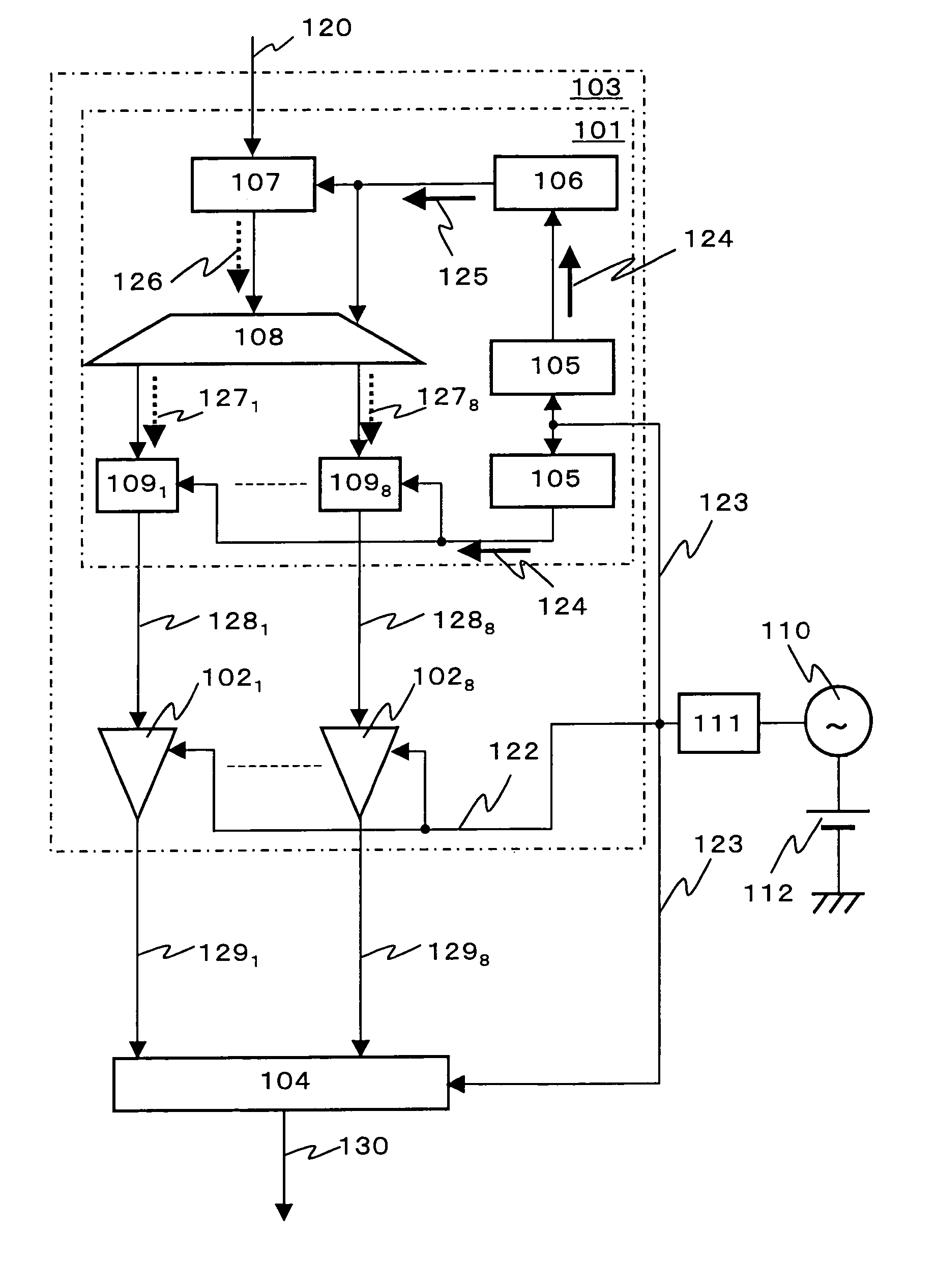
[0046]FIG. 1 is a diagram showing the overall construction of an A / D converter according to Embodiment 1. The converter has a superconducting front-end circuit 103 having an SFQ front-end circuit 101 and a superconducting amplifier circuit 102, and a semiconductor back-end circuit 104. The superconducting front-end circuit 103 oversamples an analog input signal 120, converts the analog signals to the digital data signals and makes the frequency and the voltage level of the data signals transmittable to the semiconductor back-end circuit 104. The semiconductor back-end circuit 104 signal-processes a voltage data signal 129 of the superconducting front-end circuit 103 to generate a final digital data signal 130.

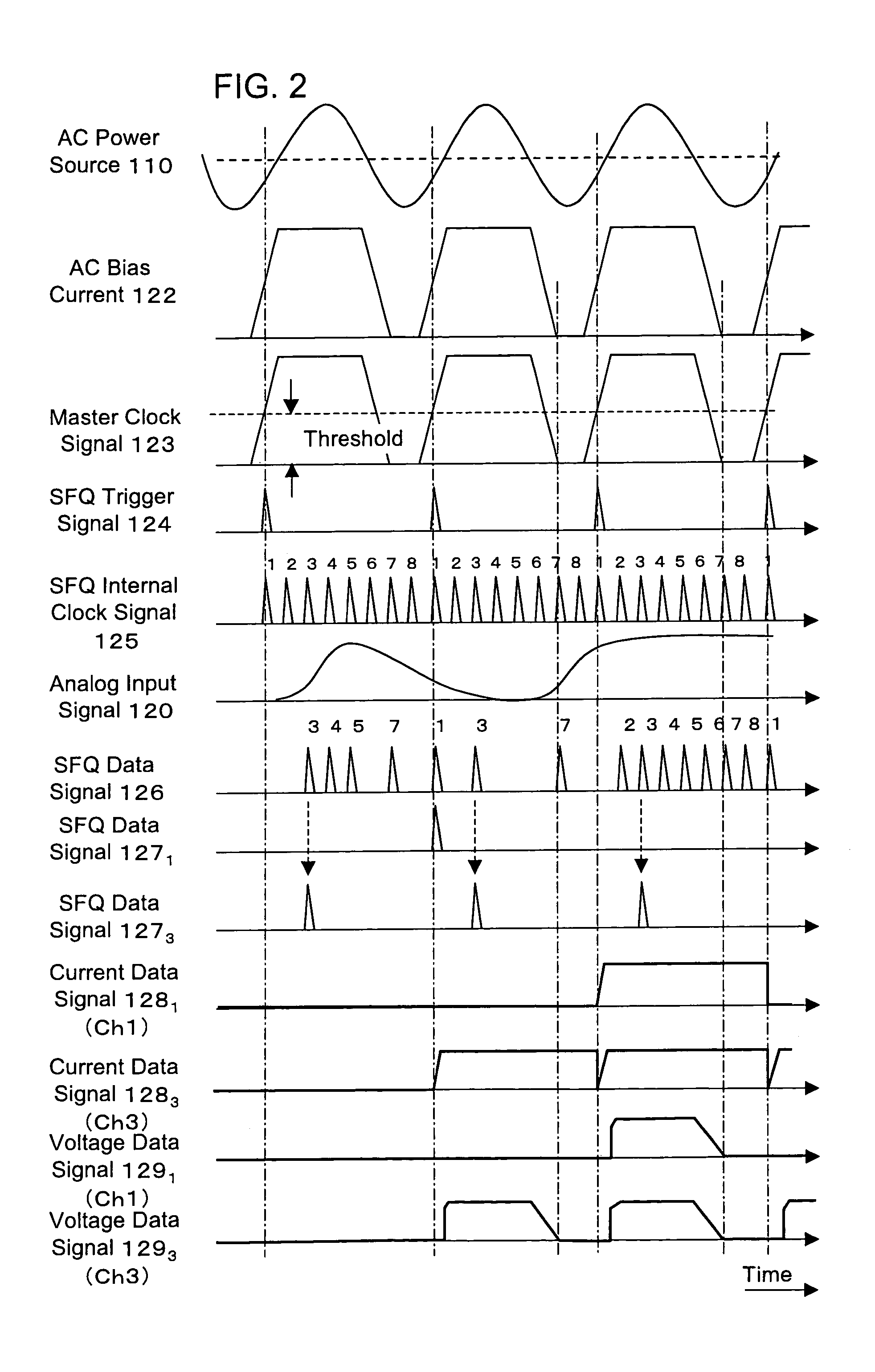
[0047]FIG. 2 is a diagram sh...

embodiment 2

[0105](Embodiment 2)

[0106]FIG. 13 is a block diagram showing, as Embodiment 2, a circuit construction when using the ring oscillator circuit 250 for the clock signal frequency multiplier circuit 106. A specific example of the ring oscillator circuit 250 is proposed in FIG. 5 of Patent Document 2. The bias current I124 supplied to the ring oscillator circuit 250, as in the 2N-bit ladder-type clock signal generating circuit 201 described in FIG. 4, is connected to the junctions of all bias current sources shown in the ring oscillator circuit 250 via the bias resistance. Here, for simplifying the drawing, the bias current I124 is introduced by the arrow. When one SFQ signal is generated by the SFQ generating circuit 105 to be inputted to the ring oscillator circuit 250, the SFQ signal is circulated on the JTL arranged in the ring form to generate an infinite number of SFQ pulse trains from the SP at any point. The pulse train is used as the SFQ internal clock signal 125. The constructi...

embodiment 3

[0111](Embodiment 3)

[0112]The memory circuit 109 and the superconducting amplifier circuit 102 of the AC-biased latching circuit described in FIG. 11 of Embodiment 1 can increase the output voltage. The AC bias current supplied to the latching circuit affects the operation of the SFQ circuit due to cross talk. FIG. 14 is an equivalent circuit diagram showing the constructions of the memory circuit 109 and the superconducting amplifier circuit 102 devised to solve-the problem of cross talk of the AC-biased latching circuit due to the AC bias current. FIG. 15 is a diagram showing an example of the layout of the main part of the circuits shown in FIG. 14. FIG. 16 is a diagram of assistance in explaining the component devices of FIG. 15.

[0113]As the circuit shown in FIG. 14 can be understood by comparison with FIG. 11, in the memory circuit 109 and the superconducting amplifier circuit 102 of Embodiment 3, a pair of the memory circuit 1091 and the superconducting amplifier circuit 1021 ...


PUM


Abstract

In an A / D converter having a single flux quantum circuit having a flux quantum as an information carrier, a superconducting amplifier circuit driven by an AC current, and a semiconductor circuit, the operations of the circuits are synchronized with each other and a data signal from the single flux quantum circuit is transmitted to the semiconductor circuit.An AC current as the power source of a superconducting amplifier circuit is inputted as a master clock signal to the single flux quantum circuit and the semiconductor circuit to synchronize the operations of the circuits with the master clock signal. The single flux quantum circuit has a clock signal frequency multiplier circuit, a demultiplexing circuit and a memory circuit.

Description

CLAIM OF PRIORITY[0001]The present application claims priority from Japanese application JP 2003-304876 filed on Aug. 28, 2003, the content of which is hereby incorporated by reference into this application.FIELD of the Invention[0002]The present invention relates to a superconducting circuit including a single flux quantum circuit and to an integrated circuit combining the superconducting circuit with semiconductor circuits.BACKGROUND OF THE INVENTION[0003]A single flux quantum (hereinafter, abbreviated as SFQ) circuit having a single flux quantum (Φ0=h / 2e=2.07×10⁻¹⁵ Weber) as an information carrier is a superconducting circuit featuring an ultrafast operation above tens of GHz (109 Hz) and a low power consumption characteristic below microwatt (μW) per gate. Based on the principle shown in Non-Patent Document 1 (IEEE Trans. on Appl. Supercond., vol. 1, No. 1 (1991) p. 1), various logic gates have been developed, and the development of practical circuits combining these with each o...

Claims


Application Information

Patent Timeline
Patent Type & Authority Patents(United States)
IPC IPC(8): H03M1/00H01L39/22G11C7/06H03M1/06H03M1/08H03M1/12
CPCG11C7/06H03M1/0624H03M1/1215
Inventor FURUTA, FUTOSHISAITOH, KAZUO
Owner HITACHI LTD
Why Eureka
Try Eureka