Illumination apparatus, exposure apparatus and device manufacturing method

a technology of exposure apparatus and manufacturing method, applied in the direction of polarising elements, printing, instruments, etc., can solve the problems of difficult design and manufacture of lenses by large na, and achieve the effect of easily correcting any deterioration of the degree of polarization without lowering the illumination efficiency

Inactive Publication Date: 2006-10-31
CANON KK
View PDF17 Cites 34 Cited by
  • Summary
  • Abstract
  • Description
  • Claims
  • Application Information

AI Technical Summary

Benefits of technology

[0008]The present invention is directed to an illumination apparatus that can set linearly polarized light in a desired direction to an arbitrary modified illumination without lowering the illumination efficiency, and easily correct any deteriorations of the degree of polarization of the linearly polarized light, an exposure apparatus having the illumination apparatus, and a device manufacturing method using the exposure apparatus.

Problems solved by technology

However, a shorter wavelength would disadvantageously reduce the transmittance through a glass material, the depth of focus decreases in inverse proportion to the NA, and a larger NA makes difficult a design and manufacture of a lens.

Method used


Image

  • Illumination apparatus, exposure apparatus and device manufacturing method
  • Illumination apparatus, exposure apparatus and device manufacturing method
  • Illumination apparatus, exposure apparatus and device manufacturing method

Examples


Embodiment Construction

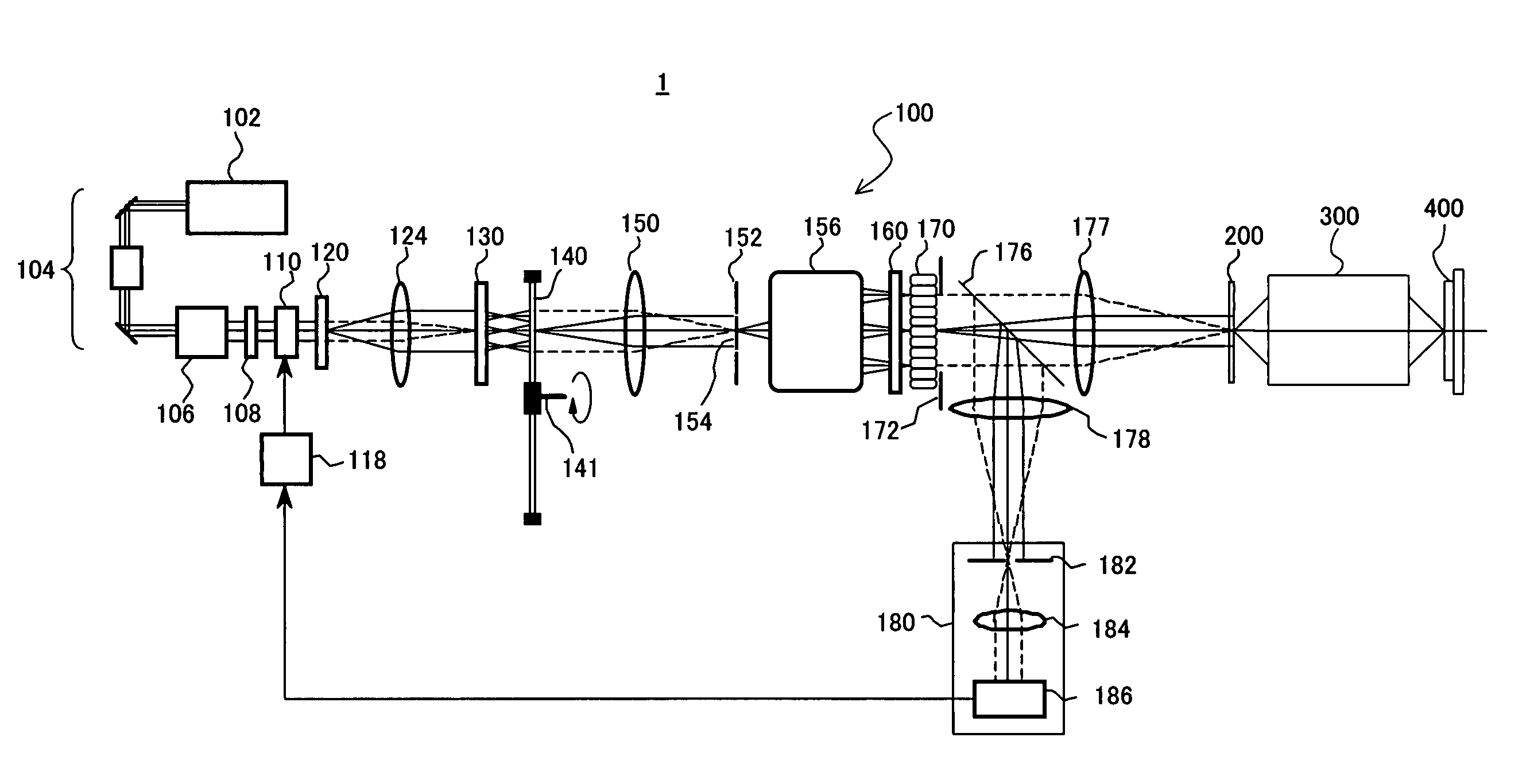
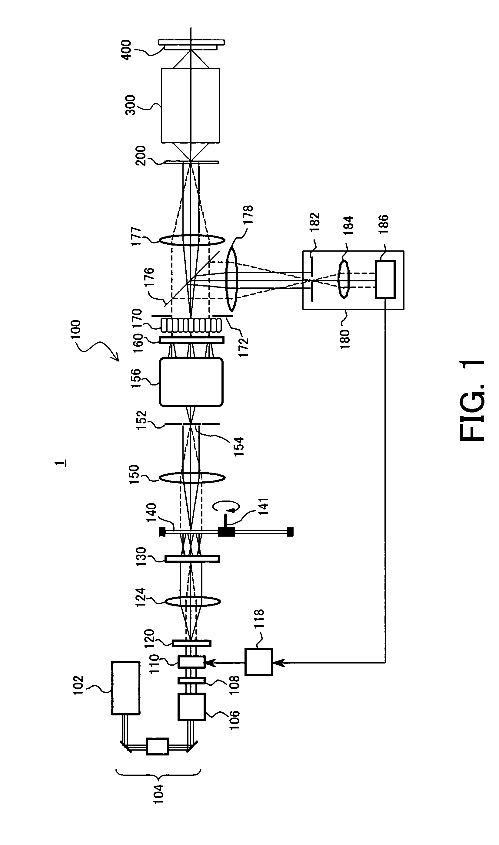
[0024]Referring now to the accompanying drawings, a description will be given of an exposure apparatus 1 mounted with an illumination apparatus 100 according to one embodiment of the present invention. Here, FIG. 1 is a schematic block diagram of the exposure apparatus 1. The exposure apparatus 1 is a projection exposure apparatus that exposes a circuit pattern of a mask 200 onto an object (plate) 400, e.g., in a step-and-repeat or a step-and-scan manner. Such an exposure apparatus is suitable to a submicron or quarter-micron lithography process, and a description will be given below of this embodiment taking a step-and-scan exposure apparatus (which is also called “a scanner”) as an example. The step-and-scan manner, as used herein, is an exposure method that exposes a mask pattern onto a wafer by continuously scanning the wafer relative to the mask, and by moving, after a shot of exposure, the wafer stepwise to the next exposure area to be shot. The step-and-repeat manner is anoth...


PUM

PropertyMeasurementUnit
wavelengthaaaaaaaaaa
center angleaaaaaaaaaa

Abstract

An illumination apparatus for illuminating a mask having a pattern, using light from a light source, includes a generating section for generating an effective light source distribution for a modified illumination to the mask, a polarization setting section for setting a predetermined polarization state in plural areas in the effective light source distribution, and an adjusting section for commonly controlling a polarization state of each area.

Description

BACKGROUND OF THE INVENTION[0001]The present invention relates generally to an illumination apparatus, and more particularly to an illumination apparatus used to expose an object, such as a single crystal substrate for a semiconductor wafer, a glass plate for a liquid crystal display (“LCD”), an exposure apparatus using the illumination apparatus and a device manufacturing method using the exposure apparatus.[0002]The recent demands for smaller and lower profile electronic apparatuses increasingly require finer processing to the semiconductor devices mounted onto these electronic devices. The photolithography process is generally used to produce highly integrated devices, such as a semiconductor device, a LCD device and a thin film magnetic head. A projection exposure apparatus is a vital apparatus to this process and exposes a pattern of a photo-mask (or reticle) onto a substrate, such as a photoresist applied silicon wafer and glass plate.[0003]The following equation gives the res...

Claims


Application Information

Patent Timeline
Patent Type & Authority Patents(United States)
IPC IPC(8): G03B27/72G03B27/54G02B5/30G02B5/32G03F7/20H01L21/027
CPCG03F7/701G03F7/70566G03F7/70125E02B13/00
Inventor TSUJI, TOSHIHIKO
Owner CANON KK
Why Eureka
Try Eureka