

Program/erase method for P-channel charge trapping memory device
a memory device and charge trapping technology, applied in the field of memory devices, can solve the problems of high power consumption, high power consumption, and change of status from “programmed” to “erased”
Active Publication Date: 2006-11-07
MACRONIX INT CO LTD
View PDF7 Cites 30 Cited by
- Summary
- Abstract
- Description
- Claims
- Application Information
AI Technical Summary
Benefits of technology
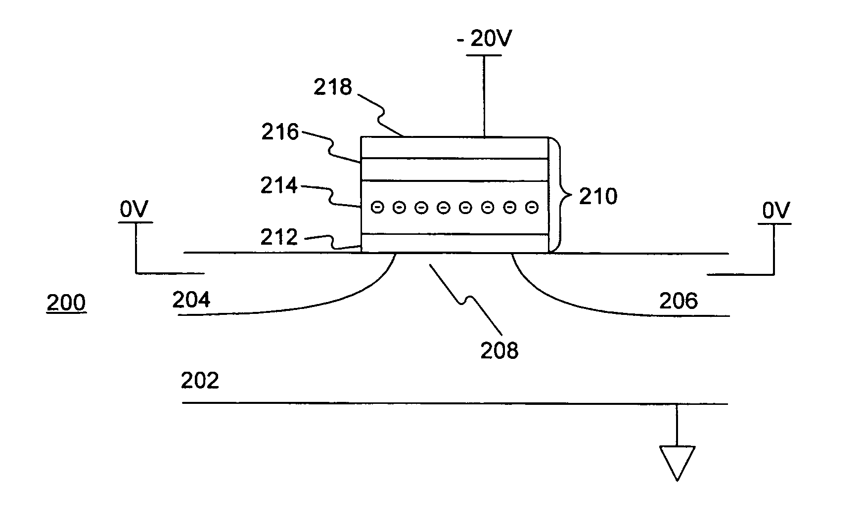
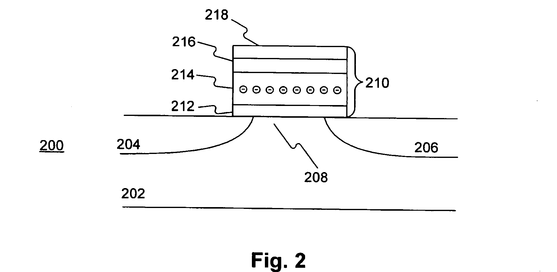
The present invention provides a memory device with improved performance and efficiency. The memory device includes a semiconductor substrate, a plurality of bit lines, and a plurality of word lines. The bit lines and word lines define a plurality of memory cells, each cell storing one bit of information. The memory device operates by applying a negative bias to the word line of the selected memory cell and a ground bias to both the first and second bit lines. The method includes selecting a memory cell by applying a turn-on voltage to all of the word lines except the word line of the selected memory cell and a ground bias to both the first and second bit lines. The memory device can store information in a faster and more efficient manner.
Problems solved by technology
However, certain problems are associated with the conventional flash memory, such as high power consumption and program and read disturbances.
High power consumption is due to high program and erasure voltages required to induce electron tunneling for program and erase operations.
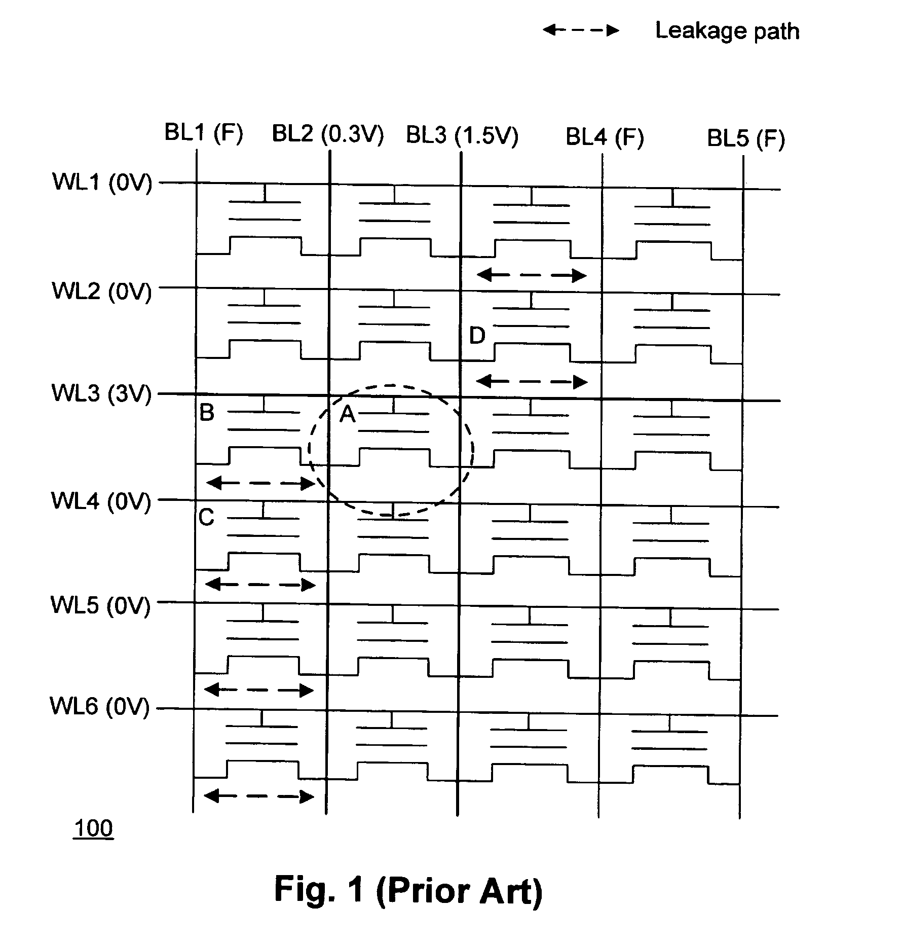
A disturbance occurs when one selected cell in the memory array is being read or programmed, another non-selected programmed memory cell sharing the same word line or bit line experiences current leakage caused by electron tunneling of the selected cell, and a loss of electrons stored in the floating gate of the non-selected memory cell may result in a change of status from “programmed” to “erased”.
In other words, a lower threshold voltage will result in a higher leakage current.
Method used
View moreImage
Smart ImageViewing Examples

Examples
first embodiment
[0026]FIG. 5 shows a memory device consistent with the present invention;
second embodiment
[0027]FIG. 6 shows a memory device consistent with the present invention; and
[0028]FIG. 7 shows a cross-sectional view of the memory device shown in FIG. 6 along line 6–6′.
Login to View More PUM
 Abstract
A method of operating a memory device is disclosed, wherein the memory device includes an n-type substrate and a plurality of memory cells formed thereon, each memory cell corresponding to a word line, a first bit line, and second bit line, and including a first bit portion and a second bit portion each for storing one bit of information. The method includes resetting a selected memory cell by applying a first negative bias to the word line of the selected memory cell and applying a ground bias to the first and second bit lines, and programming the first bit portion of the selected memory cell by applying a first positive bias to the word line of the selected memory cell, applying a second negative bias to the first bit line of the selected memory cell, and applying a ground bias to the second bit line of the selected memory cell.
Description
DESCRIPTION OF THE INVENTION[0001]1. Field of the Invention[0002]This invention is in general related to a memory device, and more particularly, to a novel flash memory device that utilizes band-to-band tunneling induced hot electron injection.[0003]2. Background of the Invention[0004]Memory devices for non-volatile storage of information have been widely in use. Examples of such memory devices include read only memory (ROM), programmable ROM (PROM), erasable programmable ROM (EPROM), electrically erasable programmable ROM (EEPROM), and flash EEPROM. A flash memory generally refers to a flash EEPROM, which may be erased in blocks of data instead of one byte at a time.[0005]A flash memory device generally includes an array of memory cells arranged in rows and columns. Each memory cell includes a MOS transistor structure having a gate, a drain, a source, and a channel defined between the drain and the source. The gate corresponds to a word line, and the drain or source corresponds to ...
Claims
Login to View More Application Information
Patent Timeline
 Patent Type & AuthorityPatents(United States)
IPC IPC(8): G11C16/04H01L21/8247H01L29/788H01L29/792H10B69/00
CPCG11C16/0475G11C16/0491G11C16/0483
InventorLUE, HANG-TING
OwnerMACRONIX INT CO LTD