Feedback system incorporating slow digital switching for glitch-free state changes

a technology of digital switching and feedback system, applied in the direction of digital transmission, pulse automatic control, oscillator generator, etc., can solve the problems of large amount of printed wiring board space, high cost of discrete implementation, and difficulty in achieving the performance required of modern systems, and the effect of increasing the vco gain

Active Publication Date: 2006-11-07
RPX CORP
View PDF21 Cites 53 Cited by
  • Summary
  • Abstract
  • Description
  • Claims
  • Application Information

AI Technical Summary

Benefits of technology

[0012]Such a capability may be accomplished in a clock and data recovery circuit, such as PLL 100, by introducing a second feedback loop which reacts to the control voltage reaching a level sufficiently different from its mid-range value by slowly adjusting additional tuning elements which, along with the tuning elements controlled by the control voltage signal, control the VCO frequency. Absent the first traditional feedback loop, a change in the VCO frequency would result, but the second feedback loop is arranged to cause a slow enough change in the VCO frequency that the first feedback loop is able to compensate for the would-be change by adjusting the control voltage quickly enough in a direction toward the mid-range value to keep the VCO frequency substantially unchanged. The second feedback loop may advantageously incorporate one or more digital control signals to affect a tuning change by changing from one state to another state. These digital signals preferably change no more than one bit at a time, and the single bit which changes is preferably caused to achieve a controlled transition time (or ramp rate) which is slow enough to cause a very gradual change in the value of the associated tuning elements. As a result, the PLL maintains lock during and after the digital signal changes state, and more importantly, maintains its phase accuracy so that the operation of the PLL, including subtle specifications such as input data jitter tolerance and jitter generation are not negatively impacted.

Problems solved by technology

However, such a discrete implementation is costly and requires a large amount of printed wiring board space, and more than likely would have difficulty achieving the performance required of modern systems while operating at an acceptable power level.
In principle this would allow a PLL to compensate for a large deviation in VCO “center frequency” without requiring a control voltage dangerously close to “running out of range.” But there are detrimental consequences of increasing the VCO gain, including danger of locking onto a harmonic, and increased noise and jitter of the system.
Moreover, with most VCO circuit structures it is difficult to arbitrarily provide an ever higher and higher tuning range and still achieve good frequency and phase stability.
In either case, such trimming is a “permanent” adjustment of the center frequency during manufacture, but it adds costly manufacturing steps to either accomplish laser trimming after wafer fabrication or to provide a semiconductor process capable of implementing flash memory structures or other kinds of programmable structures.
Moreover, such trimming is performed once during manufacture, and cannot adjust for subsequent changes in environmental conditions that the circuit may be called upon to operate under.
Such storage elements are volatile and lose stored data when the circuit loses power.
These approaches are valuable additions to the state of the art, but they cannot accommodate variations in the center frequency as environmental conditions change, as semiconductor parameters drift over time (e.g., threshold voltage shifts), or as other artifacts of component aging occur.

Method used


Image

  • Feedback system incorporating slow digital switching for glitch-free state changes
  • Feedback system incorporating slow digital switching for glitch-free state changes
  • Feedback system incorporating slow digital switching for glitch-free state changes

Examples


Embodiment Construction

)

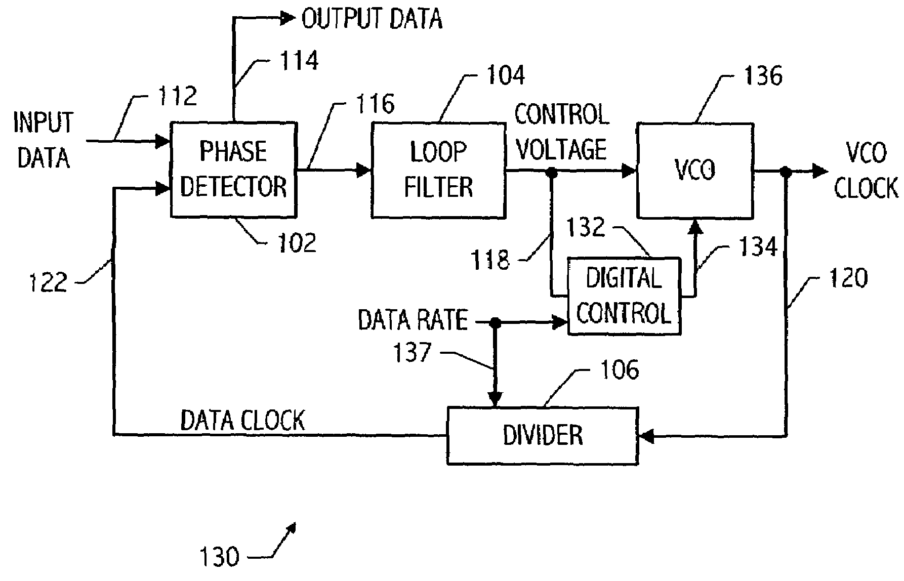
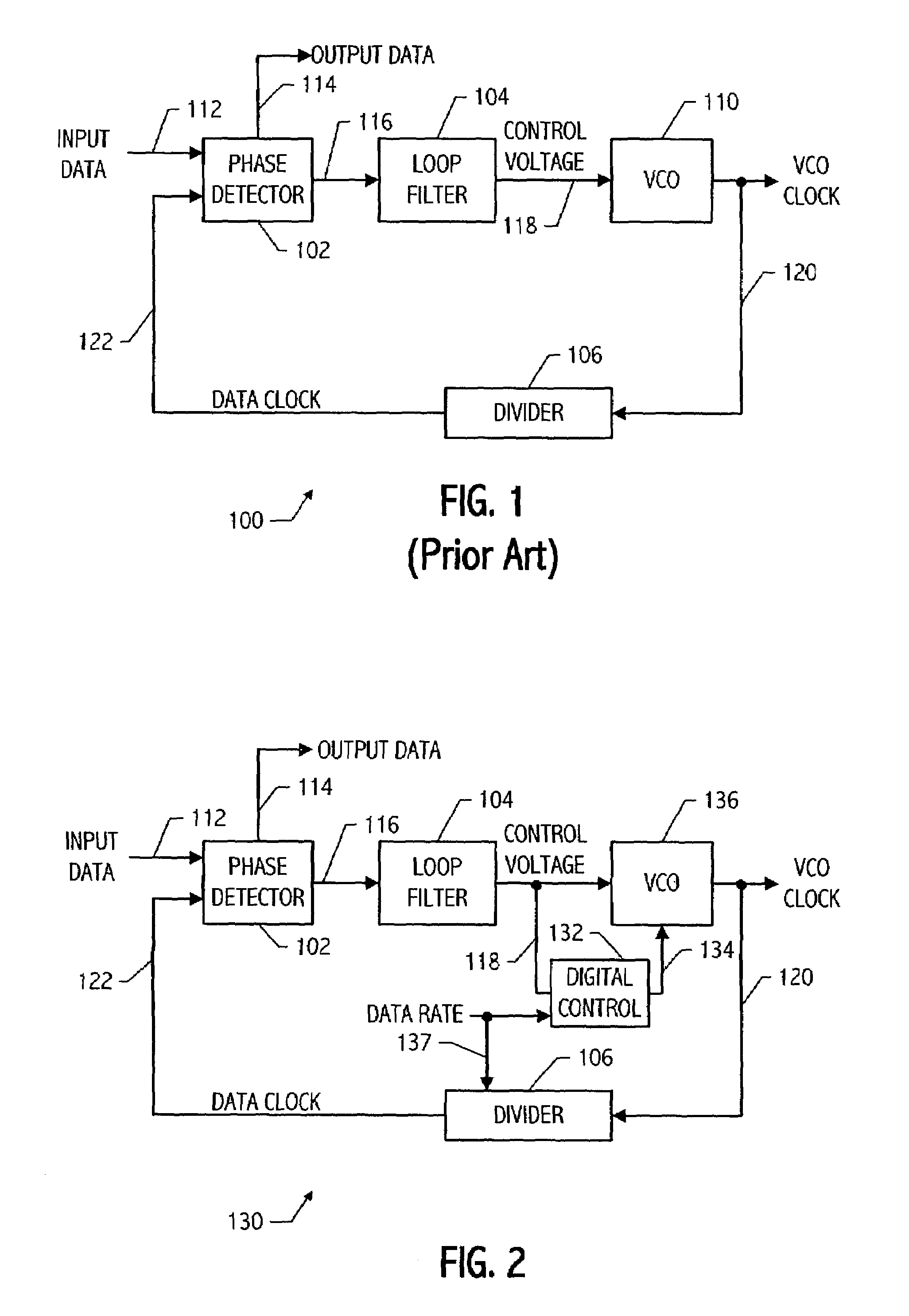
[0040]Referring now to FIG. 2, a generalized block diagram is shown of an exemplary PLL 130 configured for a clock and data recovery application which is similar in many respects to the earlier described PLL 100, but which incorporates a second feedback loop to better accommodate gradual environmental or parametric changes in the PLL. The phase locked loop 130 includes a phase detector 102 which generates on its output node 116 an error signal which is a function of the phase difference between the input data signal and the data clock signal, and which includes data retiming circuitry to generate on an output node 114 the reconstructed data, as shown. Unless the context so requires, as used herein a “phase detector” may also refer to a phase / frequency detector. A loop filter 104 filters the output of the phase detector 102 to generate a control voltage signal on node 118. A VCO 136 is provided which includes two separate control inputs (nodes 118 and 134), and which generates on it...


PUM


Abstract

A feedback system such as a phase locked loop (PLL) includes a second feedback loop which responds when a VCO control voltage is near either end of its range, by slowly adjusting additional tuning elements which control the VCO frequency. The second feedback loop is arranged to cause a slow enough change in the VCO frequency that the first traditional feedback loop adjusts the control voltage quickly enough in a direction toward its mid-range value to keep the VCO frequency substantially unchanged. The second feedback loop advantageously incorporates one or more digital control signals which preferably change no more than one bit at a time and with a controlled slow ramp rate. As a result, the PLL maintains phase accuracy so that the operation of the PLL, including subtle specifications such as input data jitter tolerance or output jitter generation when used for clock and data recovery applications, is not negatively impacted. An impedance tuning feedback system provides a resistance between two nodes which is proportional to a reference resistance, and preferably incorporates slow digital switching to result in near perturbation-free state changes over the tuning range of the resistance.

Description

CROSS-REFERENCE TO RELATED APPLICATION(S)[0001]This application is entitled to the benefit of U.S. Provisional Application No. 60 / 300,699 by Baird, et al. filed Jun. 25, 2001, the disclosure of which is incorporated herein by reference.[0002]This application is related to co-pending U.S. patent application Ser. No. 10 / 180,783 by Baird, entitled “Inpedance Tuning Circuit”, filed on even day herewith.BACKGROUND OF THE INVENTION[0003]The present invention relates to feedback control systems, and particularly to those feedback systems utilizing phase-locked loops.[0004]Feedback systems are well known in the art and are found in a multitude of different configurations. One such well-known configuration is a phase locked loop (PLL). A generalized block diagram is shown in FIG. 1 of a traditional PLL configured for a clock and data recovery application. Such a configuration may be used for recovering clock and data streams compatible with the SONET specification, as well as others. The pha...

Claims


Application Information

Patent Timeline
Patent Type & Authority Patents(United States)
IPC IPC(8): H03D3/24
CPCH03L7/099H03L7/10H03B5/1228H03B5/1212H03B5/1243H03B5/1265H03B5/124H03L2207/06H04L7/033H03B2200/0034H03L7/104
Inventor BAIRD, REX T.HUANG, YUNTENGPERROTT, MICHAEL H.
Owner RPX CORP
Why Eureka
Try Eureka