Semiconductor storage device having a function to convert changes of an electric charge amount to a current amount

a storage device and function technology, applied in the direction of semiconductor devices, transistors, electrical appliances, etc., can solve the problems of obstructing further miniaturization of the device, difficult to manufacture thin gate insulating films, and difficult two-bit operation, so as to achieve the effect of high speed

Inactive Publication Date: 2006-11-28
SHARP KK
View PDF14 Cites 9 Cited by
  • Summary
  • Abstract
  • Description
  • Claims
  • Application Information

AI Technical Summary

Benefits of technology

[0009]According to the semiconductor storage device with the above constitution, a change in the electric charge amount in the charge holding portion is converted to a current amount whereby it is operated as a memory cell. Since the two charge holding portions formed on the opposite sides of the gate electrode are formed independently of the gate insulating film, a memory function implemented by the charge holding portions and a transistor function implemented by the gate insulating film are separated. Therefore, while maintaining the sufficient memory function, the gate insulating film is made thinner, so that short channel effect can be easily prevented.
[0031]The above constitution increases the read or sense current of the semiconductor storage device so that the dispersion of read or sense current may be controlled. Therefore, the readout operation of the semiconductor storage device can be made at a higher speed.

Problems solved by technology

This makes it difficult to manufacture thinner gate insulating films.
Also, in the above nonvolatile memory, as the channel length is shortened, the two memory holding portions 907, 908 in one transistor interfere with each other, which makes two-bit operation difficult.
This obstructs further miniaturization of the devices.

Method used


Image

  • Semiconductor storage device having a function to convert changes of an electric charge amount to a current amount
  • Semiconductor storage device having a function to convert changes of an electric charge amount to a current amount
  • Semiconductor storage device having a function to convert changes of an electric charge amount to a current amount

Examples


embodiment 1

[0058](Embodiment 1)

[0059]Before describing a memory device constituting a semiconductor storage device of the present invention, a basic structure that is a premise of a memory device to which this invention is applied will be described first with reference to FIGS. 9 and 10.

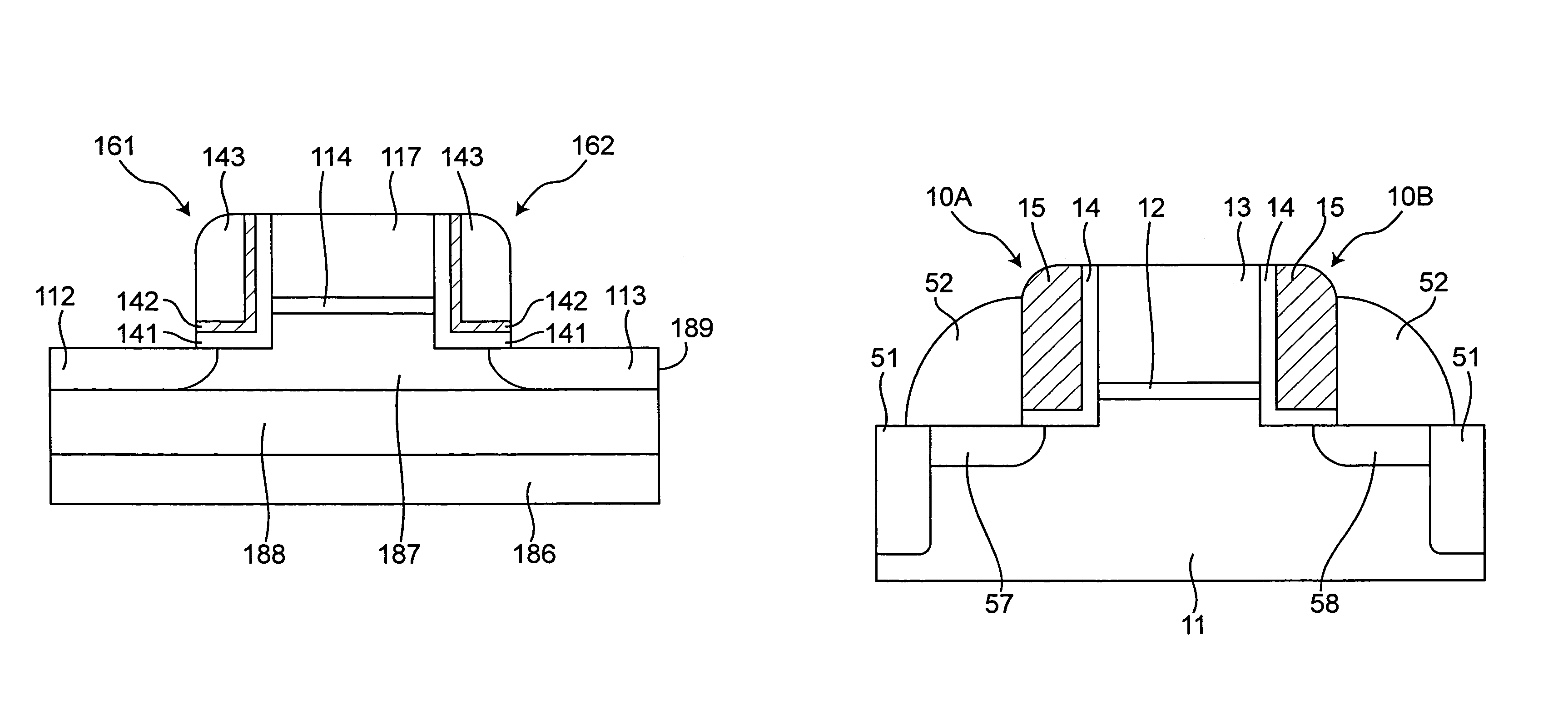
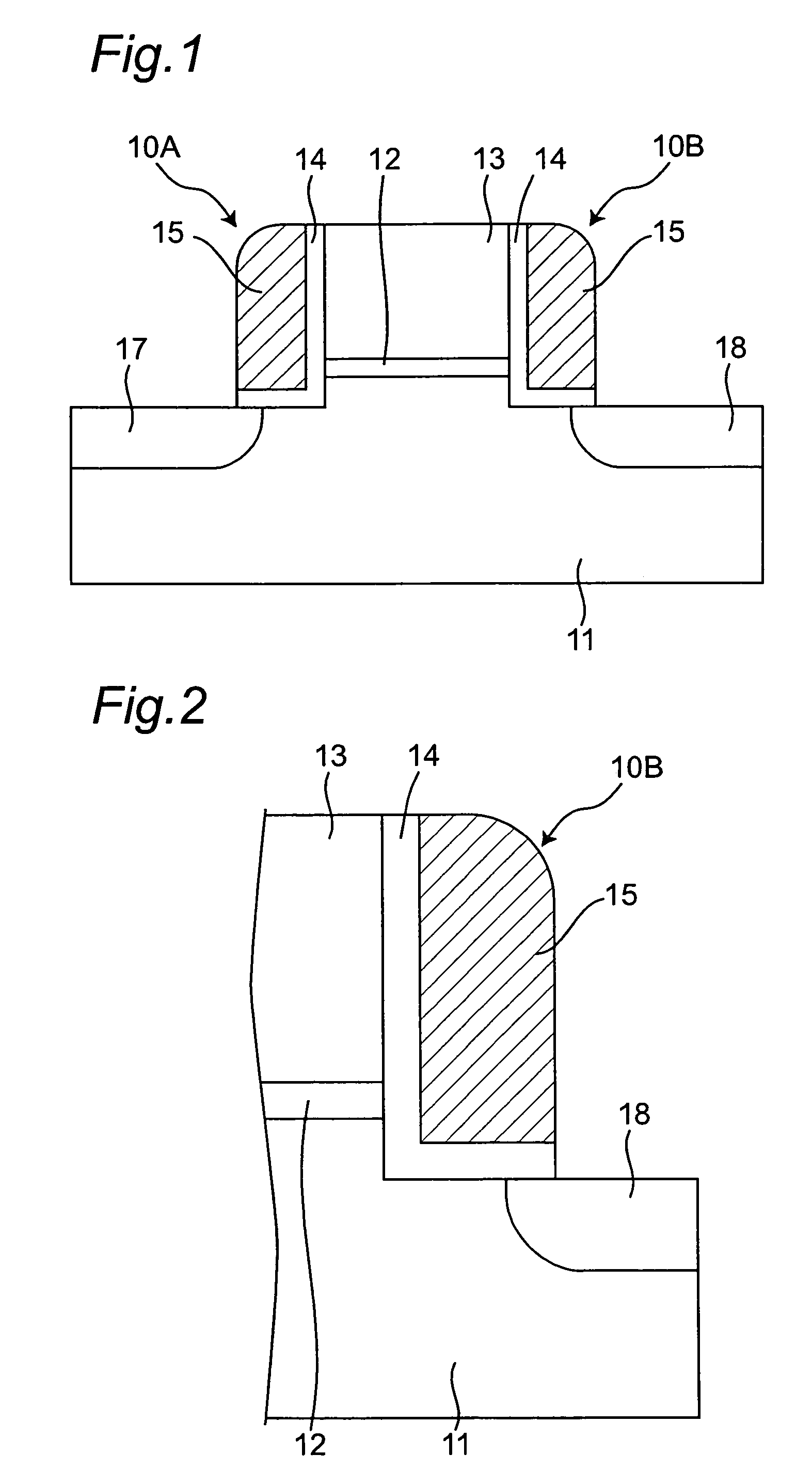
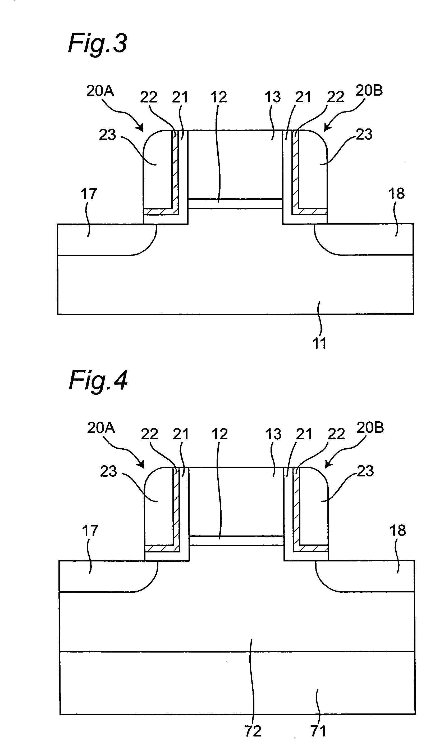
[0060]FIG. 9 is a schematic cross-sectional view of a memory device. In the memory device as a nonvolatile memory cell capable of storing two bits, as shown in FIG. 9, a gate electrode 13 having a gate length similar to those of normal transistors is formed on a semiconductor substrate 11 that is one example of the first conductivity type (e.g., one of the P type or N type) semiconductor part, with a gate insulating film 12 therebetween. Charge holding portions 10A, 10B in the shape of side wall spacer are formed on side surfaces, or side walls of the gate insulating film 12 and the gate electrode 13 that are stacked. That is, one of the charge holding portions 10A and 10B is disposed on one of the side walls, ...

embodiment 2

[0095](Embodiment 2)

[0096]In a memory device (semiconductor memory storage device) of Embodiment 2, as shown in FIG. 11, each charge holding portion 161, 162 is composed of a region for holding electric charges and a region for obstructing release or escape of electric charges. The region for holding electric charges is a region that stores electric charges, which may be a film having a function of holding electric charges. The region for obstructing release of electric charges may be given by a film having a function of obstructing release of electric charges.

[0097]The charge holding portion 161, 162 has, for example, an ONO (Oxide Nitride Oxide) structure. More specifically, the charge holding portions 161, 162 are each structured in the state that a silicon nitride film 142 is interposed between a silicon oxide film 141 and a silicon oxide film 143. Here, the silicon nitride film 142 implements a function of holding electric charges. The silicon oxide films 141, 143 implement a f...

embodiment 3

[0115](Embodiment 3)

[0116]In a memory device of Embodiment 3, a silicon nitride film (charge holding film) 142 in the charge holding portion 161, 162 has an approximately uniform film thickness as shown in FIG. 16. Further, the charge holding film 142 includes a portion (region 181) disposed approximately parallel to a top surface of the gate insulating film 114 and a portion (region 182) approximately parallel to a side surface of the gate electrode 117.

[0117]When a positive voltage is applied to the gate electrode 117, an electric line of force in the charge holding portion 162 passes the silicon nitride film 142 totally twice (through the first portion 181 and the second portion 182) as shown with arrow 183. It is noted that when a negative voltage is applied to the gate electrode 117, the direction of the electric line of force is reversed.

[0118]Herein, a relative permittivity, or dielectric constant of the silicon nitride film 142 is approx. 6, while a dielectric constant of si...


PUM


Abstract

In a semiconductor storage device, a gate insulating film and a gate electrode are laid on a first conductivity type semiconductor substrate, and charge holding portions are formed on both sides of the gate electrode. Second conductivity type first and second diffusion layer regions are formed in regions of the semiconductor substrate corresponding to the charge holding portions. The charge holding portions are each structured so as to change, in accordance with an electric charge amount held in the charge holding portions, a current amount flowing from one of the second conductivity type diffusion layer regions to the other of the diffusion layer regions through a channel region when voltage is applied to the gate electrode. Part of each charge holding portion is present below an interface of the gate insulating film and the channel region.

Description

[0001]This application is the U.S. National Phase of International Application PCT / JP2003 / 012583, filed Oct. 1, 2003, which designated the U.S. PCT / JP2003 / 012583 claims priority to JP Patent Applications No. 2002-296001, filed Oct. 9, 2002 and No. 2003-136453, filed May 14, 2003. The entire contents of these applications are incorporated herein by reference.TECHNICAL FIELD[0002]This invention relates to a semiconductor storage device. In particular, it relates to a semiconductor storage device having a field-effect transistor having a function to convert changes of an electric charge amount to a current amount.BACKGROUND ART[0003]Conventionally, there has been a nonvolatile memory capable of storing two bits by one field-effect transistor (e.g., see JP-2001-512290 A, published Aug. 21, 2001). The structure of this nonvolatile memory and the principle of its write (program) operation will be described hereinbelow.[0004]As shown in FIG. 25, this memory is composed of a gate electrode ...

Claims


Application Information

Patent Timeline
Patent Type & Authority Patents(United States)
IPC IPC(8): H01L29/792H01L21/8247H01L21/28H01L21/336H01L27/115H01L29/788
CPCH01L21/28273H01L21/28282H01L29/7923H01L29/66833H01L29/7887H01L29/66825H01L29/40114H01L29/40117
Inventor IWATA, HIROSHISHIBATA, AKIHIDE
Owner SHARP KK
Why Eureka
Try Eureka