SONOS memory with inversion bit-lines

Active Publication Date: 2006-12-19
LONGITUDE FLASH MEMORY SOLUTIONS LTD
View PDF4 Cites 33 Cited by
  • Summary
  • Abstract
  • Description
  • Claims
  • Application Information

AI Technical Summary

Benefits of technology

[0014]In a further embodiment of the present invention, at least one of the top dielectric, the charge trapping material, and the bottom d

Problems solved by technology

Such higher number of contacts formed within the core region disadvantageously increases the area of the core region in the

Method used


Image

  • SONOS memory with inversion bit-lines
  • SONOS memory with inversion bit-lines
  • SONOS memory with inversion bit-lines

Examples


Example

[0029]The figures referred to herein are drawn for clarity of illustration and are not necessarily drawn to scale. Elements having the same reference number in FIGS. 1, 2, 3, 4, 5, 6, 7, 8, 9, 10, 11, and 12 refer to elements having similar structure and function.

DETAILED DESCRIPTION

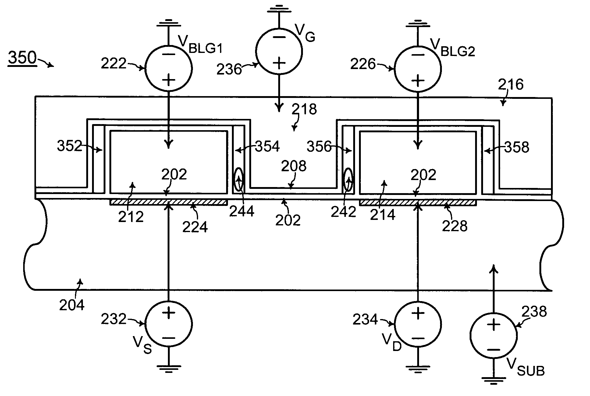
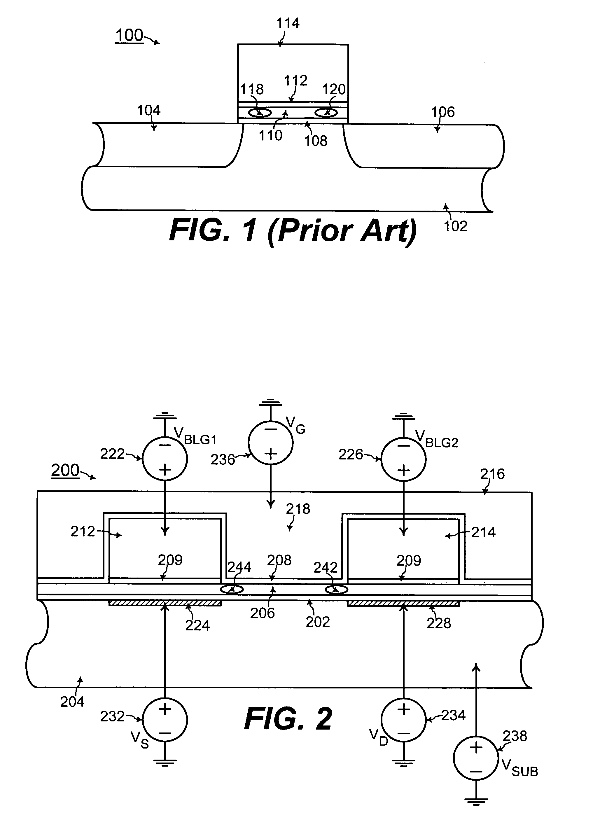
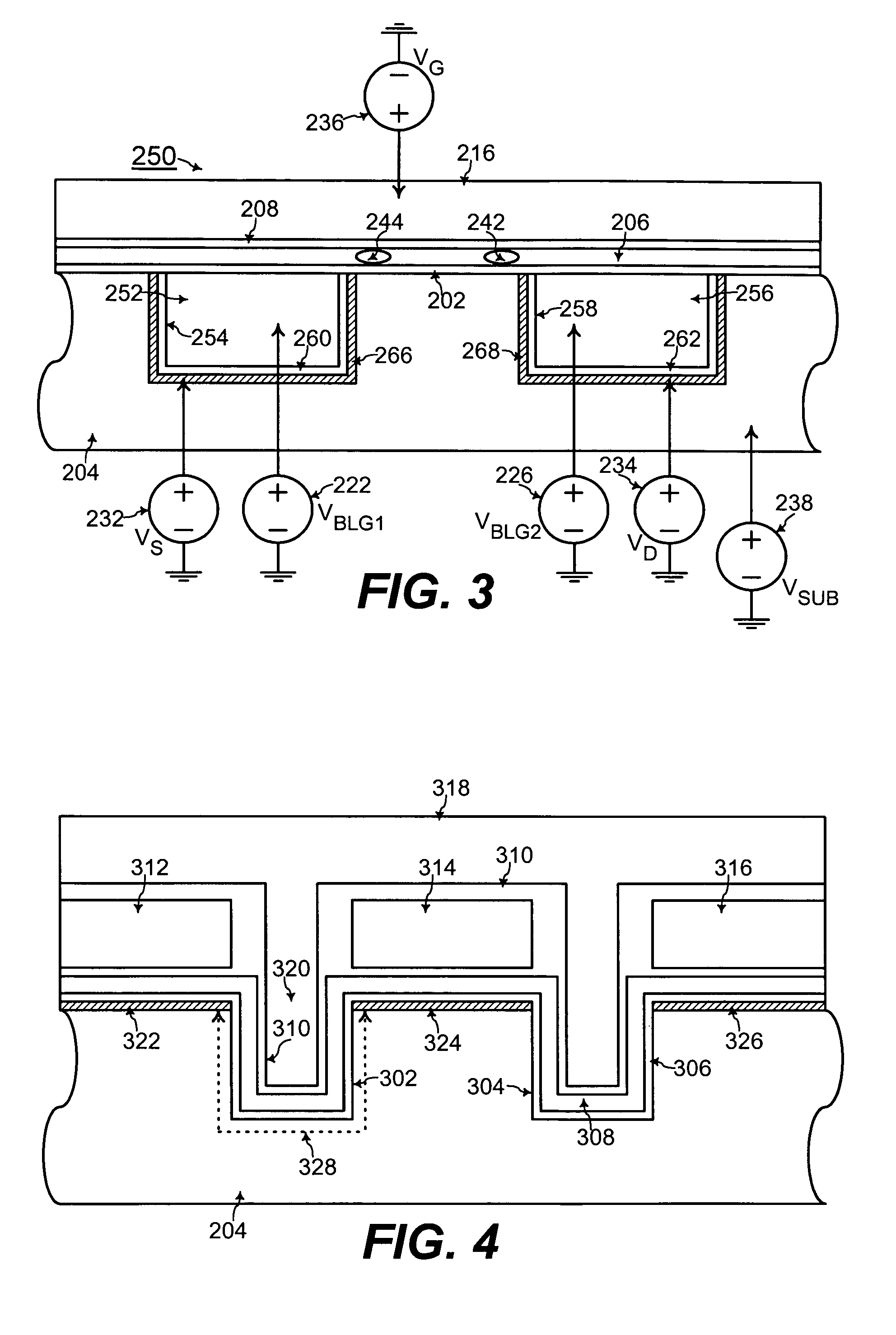
[0030]FIG. 2 shows a cross-sectional view of a SONOS memory cell 200 with inversion bit-lines according to an embodiment of the present invention. The SONOS memory cell 200 includes a bottom dielectric 202 formed on a semiconductor substrate 204. The bottom dielectric 202 is comprised of silicon dioxide (SiO2) or a high-k dielectric having a dielectric constant higher than that of silicon dioxide (SiO2), in one embodiment of the present invention. The semiconductor substrate 204 may be a P-well formed in a silicon wafer, in one embodiment of the present invention.

[0031]A charge trapping material 206 is formed on the bottom dielectric 202. The charge trapping material 206 is comprised of silicon nitride (...


PUM


Abstract

A SONOS memory cell, formed within a semiconductor substrate, includes a bottom dielectric disposed on the semiconductor substrate, a charge trapping material disposed on the bottom dielectric, and a top dielectric disposed on the charge trapping material. Furthermore, the SONOS memory cell includes a word-line gate structure disposed on the top dielectric and at least one bit-line gate for inducing at least one inversion bit-line within the semiconductor substrate.

Description

TECHNICAL FIELD[0001]The present invention relates generally to non-volatile memory, and more particularly, to SONOS (semiconductor oxide nitride oxide semiconductor) memory with inversion bit-lines for eliminating diffusion bit-lines.BACKGROUND OF THE INVENTION[0002]FIG. 1 shows a conventional SONOS (semiconductor oxide nitride oxide semiconductor) memory cell 100 formed on a semiconductor substrate 102. The SONOS memory cell 100 includes a source bit-line junction 104 and a drain bit-line junction 106 formed within the semiconductor substrate 102. For example, the semiconductor substrate 102 may be a P-well formed within a silicon wafer with the bit-line junctions 104 and 106 having N-type dopant therein.[0003]The SONOS memory cell 100 also includes a stack of a bottom dielectric 108 (typically comprised of silicon dioxide SiO2), an intermediate dielectric 110 (typically comprised of silicon nitride SiN), and a top dielectric 112 (typically comprised of silicon dioxide SiO2). A co...

Claims


Application Information

Patent Timeline
IPC IPC(8): H01L29/72
CPCH01L27/115H01L27/11568H01L29/66833H01L29/792G11C16/0475H10B69/00H10B43/30
Inventor SHIRAIWA, HIDEHIKOPARK, JAEYONGTORII, SATOSHIARAKAWA, HIDEKIYANO, MASARU
Owner LONGITUDE FLASH MEMORY SOLUTIONS LTD
Why Eureka
Try Eureka