
High pressure sensor comprising silicon membrane and solder layer

a technology of solder layer and silicon membrane, applied in the direction of fluid pressure measurement, fluid pressure measurement by electric/magnetic elements, instruments, etc., to achieve the effect of high degree of integration of the devi

Inactive Publication Date: 2006-12-26
ROBERT BOSCH GMBH
View PDF16 Cites 21 Cited by
  • Summary
  • Abstract
  • Description
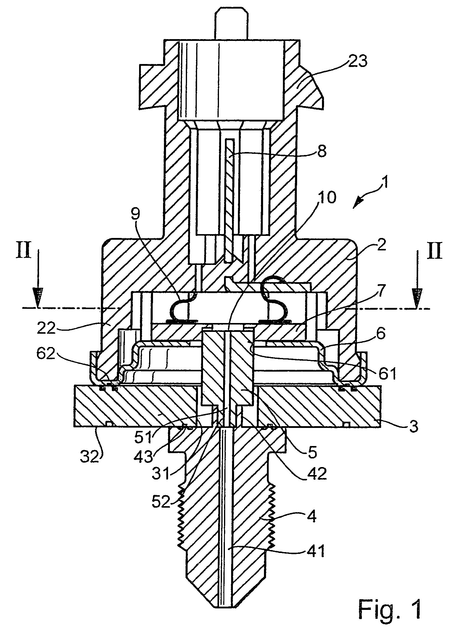
  • Claims
  • Application Information

AI Technical Summary

Benefits of technology

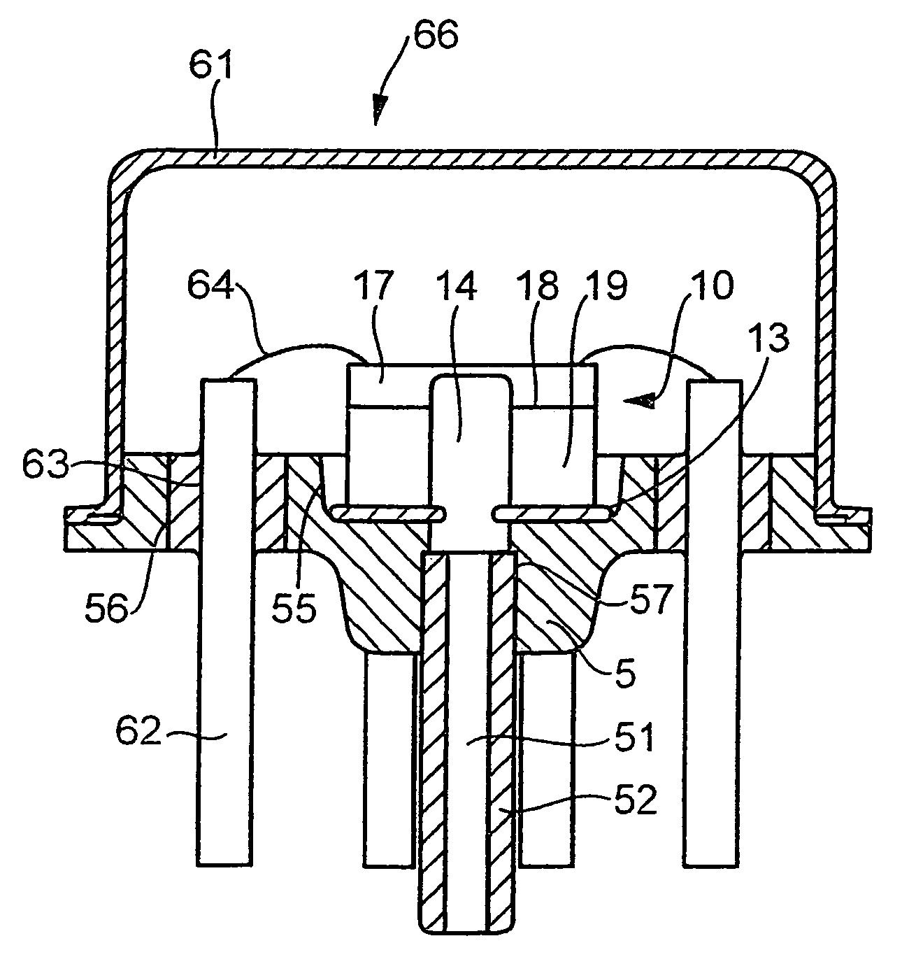
[0004]An embodiment of a device according to the present invention for measuring pressure may allow use of a pressure transducer including a semiconductor chip, on whose upper side are formed sensor elements and, for example, additionally, an evaluation circuit as an integrated circuit, for measuring high pressure above 70 bar. The degree of complexity pursued in other systems for insulating the sensor elements from the metallic pressure-measuring cell in the case of conventional high-pressure sensors may be avoided. By combining the evaluation circuit and sensor elements on the semiconductor chip, a high degree of integration of the device may be achieved. In this context, by directly soldering the semiconductor chip, using an edge area surrounding a cutout in the semiconductor chip, onto a support part provided with a first pressure-channel section, the first pressure-channel section and the cutout being interconnected, a connection resistant to high pressure may be produced between the semiconductor chip and the support part.
[0005]The pressure transducer may be formed in one piece from a semiconductor material such as silicon. A stack assembly may be used that includes a first semiconductor structure, provided with the sensor diaphragm and the sensor elements, and a second semiconductor structure fixedly joined thereto via a connection zone and soldered onto the support part. The second semiconductor structure largely prevents thermomechanical stress loads from reaching and damaging the sensor elements. The reliability and service life of the device is thereby increased. The first semiconductor structure and the second semiconductor structure may be made of silicon. The connection zone may be made of a eutectic zone of gold and silicon.
[0006]To prevent thermal stresses between the semiconductor chip and the support part, the solder layer has a lower thermal expansion coefficient than tin-lead solder, which is better adapted to the semiconductor material. For example, the use of AuSn20-solder may be advantageous.
[0008]The cutout in the semiconductor pressure transducer may be formed by reactive ion etching (trench etching) on the pressure transducer. In this manner, sharp transitions and bends in the semiconductor pressure transducer, at which stresses form in response to high pressure loads which lead to the formation of fractures, are avoided.
[0009]The device may include a sensor housing; and affixed as a separate component to an outer side of a first sensor-housing part of the sensor housing that is provided with a through hole is a connection piece covering the through hole, and the support part positioned in the sensor housing is connected to the connection piece through the through hole, for example, by laser welding, since thermomechanical stresses between the connection piece and the support part may thereby be considerably reduced.

Problems solved by technology

However, such pressure sensors are only used for measuring relatively small pressures below 70 bar, since the mechanical stresses acting at greater pressures lead to fractures in the glass or silicon chip.

Method used


Image

  • High pressure sensor comprising silicon membrane and solder layer
  • High pressure sensor comprising silicon membrane and solder layer
  • High pressure sensor comprising silicon membrane and solder layer

Examples


Embodiment Construction

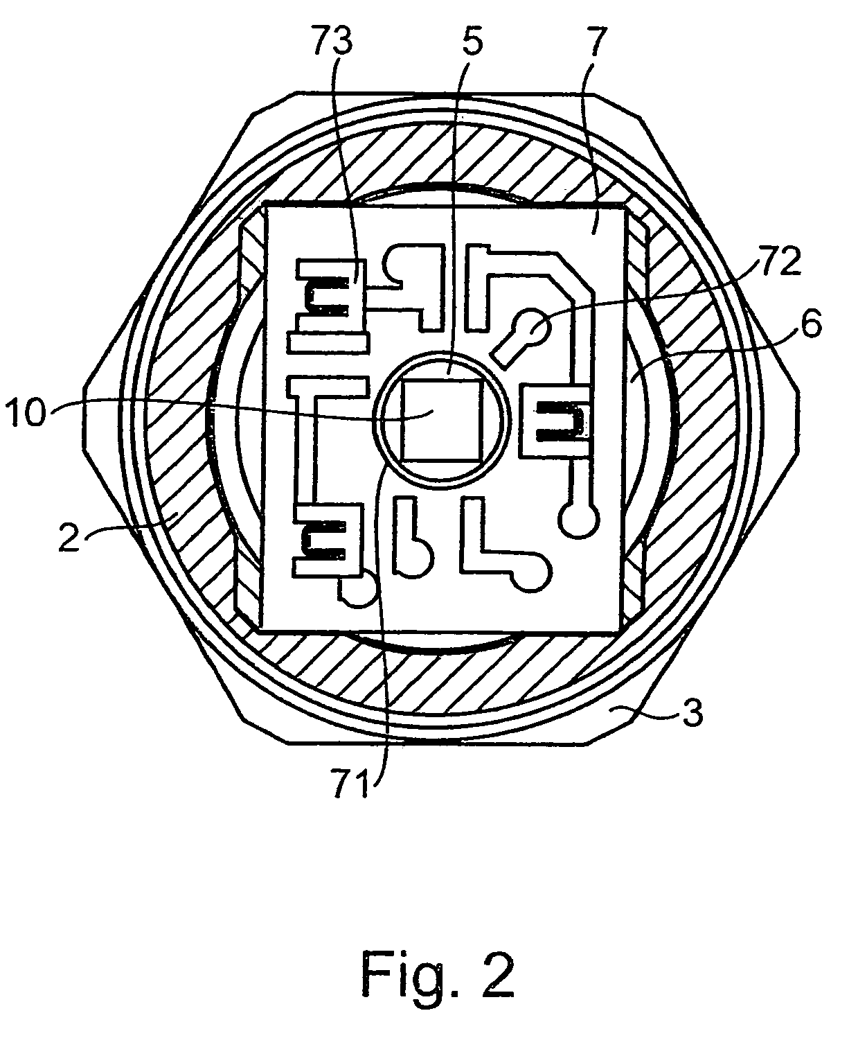
[0018]FIGS. 1 and 2 show a first exemplary embodiment of the device according to the present invention for measuring pressure. A semiconductor pressure transducer 10 is soldered onto a pedestal-type support part 5. An enlarged detail view of the semiconductor pressure transducer soldered onto pedestal 5 is shown in FIG. 3. Semiconductor pressure transducer 10 may be formed as a silicon chip and may be provided with sensor elements 12 on upper side 15. A central section on the upper side which stretches over a cutout 14 introduced into the lower side is used as sensor diaphragm 11, sensor elements 12 sensing deformations of thin sensor diaphragm 11 resulting from a compressive load of the same. In addition to sensor elements 12, an evaluation circuit may also be arranged on upper side 15 of semiconductor pressure transducer 10 around sensor diaphragm 11. Cutout 14 may be introduced into the pressure transducer by reactive ion etching (trench etching), which means gentle transitions d...


PUM


Abstract

A device for measuring pressure, e.g., for measuring high pressure, including a pressure transducer that is arranged in a housing and includes sensor elements and a sensor diaphragm on a first side, and on a second side opposite the first side is provided with a cutout that extends from the second side to the sensor diaphragm. The pressure transducer is formed as a semiconductor pressure transducer and, with an edge area of the second side surrounding the cutout, is directly soldered onto a support part, provided with a first pressure-channel section, with the aid of a solder layer in such a manner that the first pressure-channel section and the cutout are interconnected.

Description

FIELD OF THE INVENTION[0001]The present invention relates to a device for measuring pressure.BACKGROUND INFORMATION[0002]A device for measuring pressure is described in, for example, German Published Patent Application No. 100 14 992. This high-pressure sensor uses a metal pressure-measuring cell, provided with a recess, as a pressure transducer. Sensor elements and a measuring diaphragm are formed on one side of the metallic pressure-measuring cell. With the opposite second side, the pressure-measuring cell is welded onto a connection piece of the sensor device. An evaluation circuit is arranged on a separate printed circuit board or a hybrid, and is electrically connected to the sensor elements on the upper side of the pressure-measuring cell. High pressures above 140 bar may also be measured using such a device.[0003]Furthermore, in German Published Patent Application No. 197 31 420, for instance, a device is described for measuring pressure including a silicon chip as a semicond...

Claims


Application Information

Patent Timeline
IPC IPC(8): G01L9/00G01L1/00G01L7/08G01L19/14G01L23/24H01L29/84
CPCG01L19/0084G01L19/14G01L19/143G01L19/147H01L2224/48091H01L2924/10155H01L2924/00014G01L9/00
Inventor MAST, MARTIN
Owner ROBERT BOSCH GMBH
Learn More