Semiconductor device

a technology of semiconductor devices and shielding films, applied in semiconductor devices, semiconductor/solid-state device details, electrical devices, etc., can solve the problems of low film density weak cu wiring, and noticeable signal transmission delay disadvantages, etc., to achieve enhanced adhesiveness of diffusion prevention insulation films and conductive layers, the effect of reducing the capacity of the signal transmission delay

Active Publication Date: 2006-12-26
SONY CORP +1
View PDF10 Cites 4 Cited by
  • Summary
  • Abstract
  • Description
  • Claims
  • Application Information

AI Technical Summary

Benefits of technology

[0012]According to a semiconductor device as above, since the diffusion prevention insulation film is configured by sandwiching between a lowermost layer and an uppermost layer a middle layer having a lower relative dielectric constant than those of the lowermost layer and the uppermost layer, a low dielectric constant can be attained in the diffusion prevention insulation film, so that a capacity thereof can be reduced even in the case where the diffusion prevention insulation film is made thinner as the semiconductor device becomes finer. Also, the lowermost layer and the uppermost layer of the diffusion prevention insulation film have a higher relative dielectric constant than that of the middle layer, so that the film density becomes higher than that of the middle layer. As a result, the lowermost layer formed in a state of contacting an insulation film including a conductive layer obtains high film density, so that adhesiveness of the diffusion prevention insulation film and the conductive layer is enhanced. Also, the uppermost layer composing the uppermost portion of the diffusion prevention insulation film becomes hard to be permeated by water and oxygen from the air and the interlayer insulation film as the upper layer due to the high film density, so that oxidization of the conductive layer is prevented. Furthermore, as a result that the film density of the lowermost layer and the uppermost layer is made high, strength of the diffusion prevention insulation film itself can be also maintained.
[0013]As explained above, according to the semiconductor device of the present invention, even in the case where the diffusion prevention insulation film is made thin, a capacity of a diffusion prevention insulation film is reduced, so that a capacity between wiring layers can be reduced. Also, as a result that adhesiveness between the diffusion prevention insulation film and a conductive layer becomes high, arising of voids caused because metal elements in the conductive layer become easy to move is prevented, so that the EM resistance and the SM resistance of the conductive layer can be improved and wiring reliability can be improved. Furthermore, since oxidization of the conductive layer is prevented, wiring resistance can be maintained low. Also, because strength of the diffusion prevention insulation film itself is maintained, property of withstand voltage, such as TDDB, can be also improved.
[0014]As a result, a capacity between wiring layers can be reduced, wiring reliability and property of withstand voltage of the diffusion prevention insulation film are improved, and wiring resistance can be maintained low, so that a high-speed CMOS device having high density can be realized. Accordingly, performance of computers, game machines and mobile products can be remarkably improved.

Problems solved by technology

This is because disadvantages of a signal transmission delay have become noticeable as semiconductor elements become finer.
However, in a semiconductor device as above, a relative dielectric constant of a diffusion prevention insulation film is high, so that it is necessary to lower the dielectric constant not only of the interlayer insulation film but of the diffusion prevention insulation film to reduce the capacity between wiring layers as the semiconductor device becomes finer.
However, when the dielectric constant of the diffusion prevention insulation film is made lower, film density of the diffusion prevention insulation film becomes low, so that a surface reaction with the Cu wiring becomes weak and adhesiveness of the diffusion prevention insulation film and the Cu wiring declines.
Consequently, voids arise as a result that Cu easily moves and disadvantages of declining the wiring reliability arise, such that electro migration (EM) resistance and stress migration (SM) resistance decline.
Also, as a result that the film density of the diffusion prevention insulation film declines, there is a disadvantage that oxygen and water from the air or the interlayer insulation film provided as an upper layer of the diffusion prevention insulation film permeate the diffusion prevention insulation film, and the Cu wiring as the lower layer is oxidized to increase the wiring resistance.
Furthermore, due to a decline of the film density, it is liable that strength of the diffusion prevention insulation film itself declined and resistance properties, such as time dependence on dielectric breakdown (TDDB), decline.

Method used


Image

  • Semiconductor device
  • Semiconductor device
  • Semiconductor device

Examples


example 1

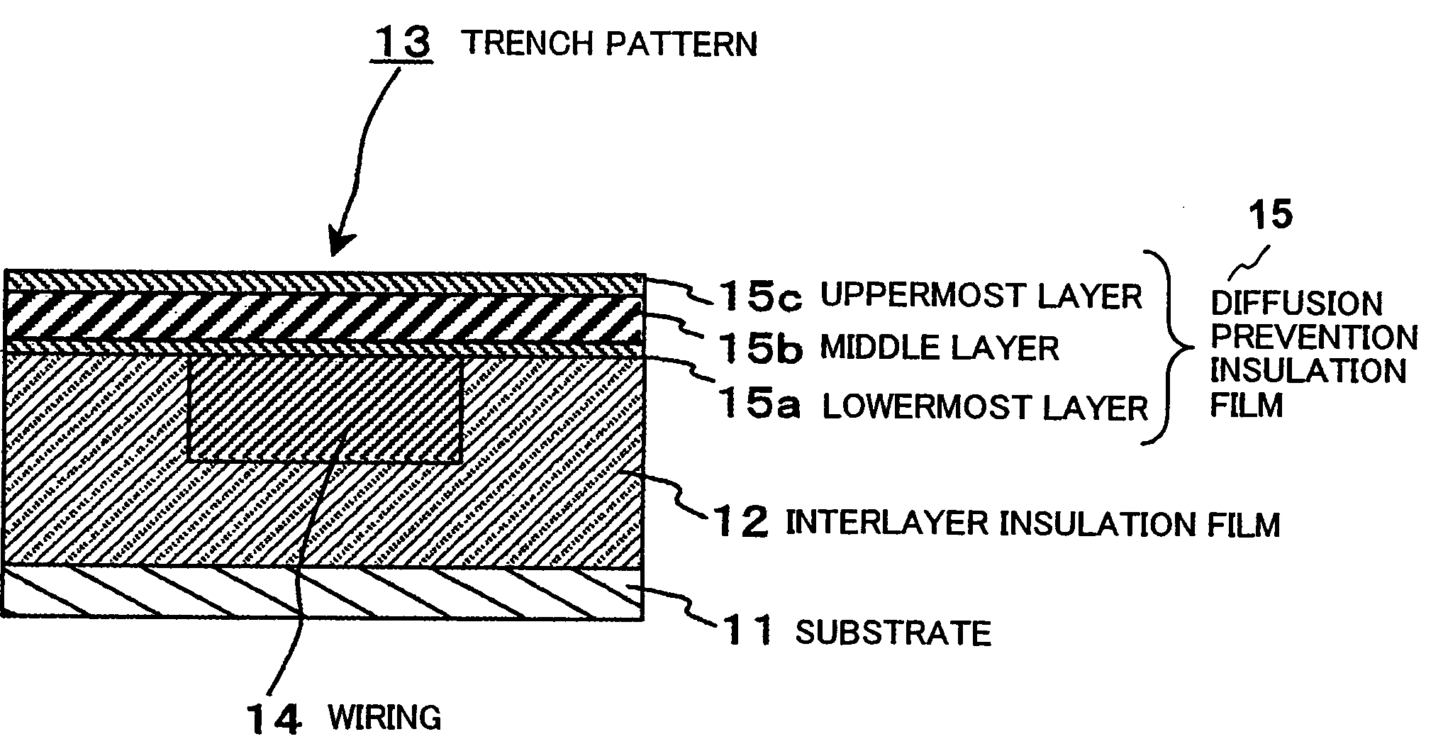
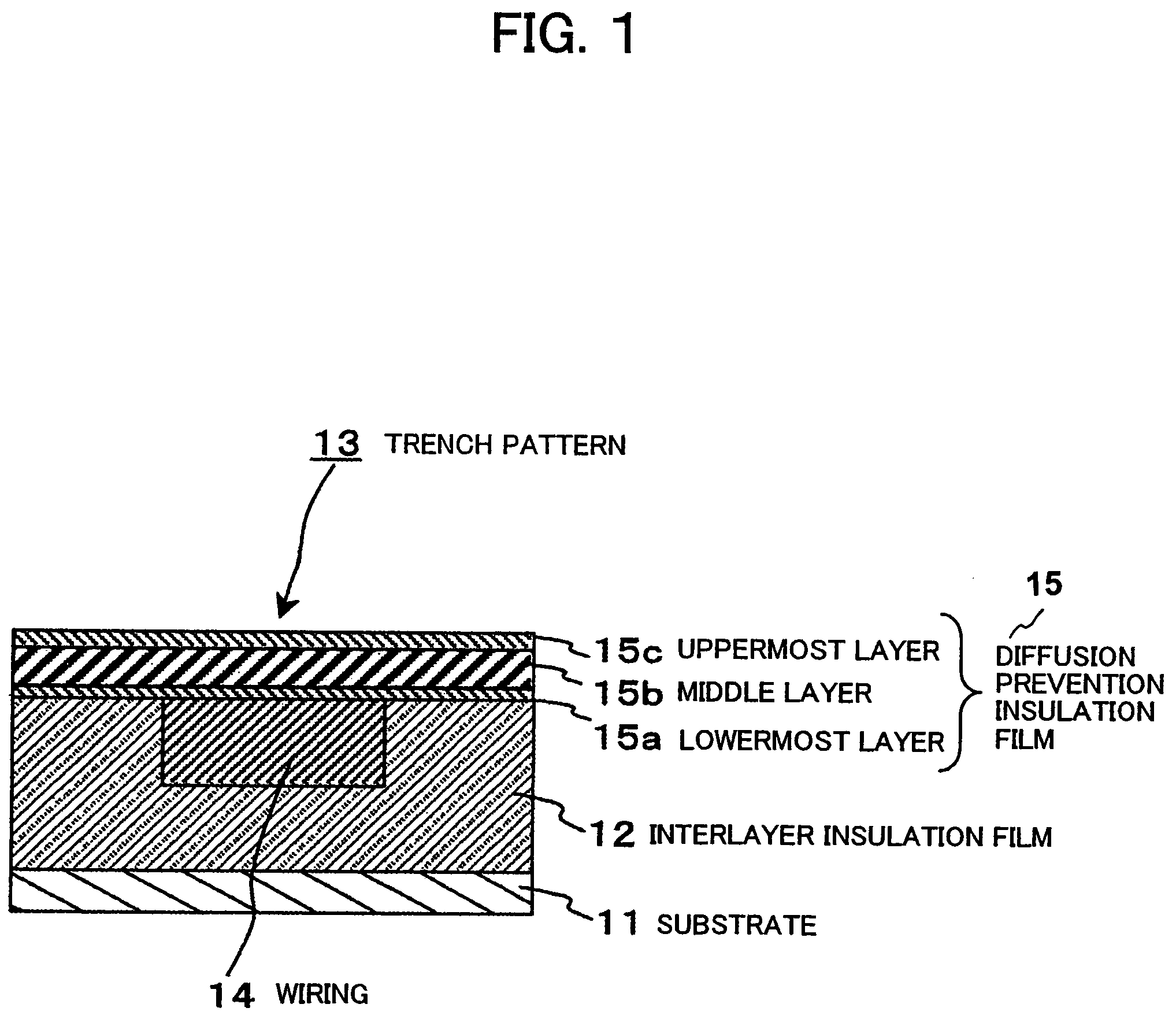
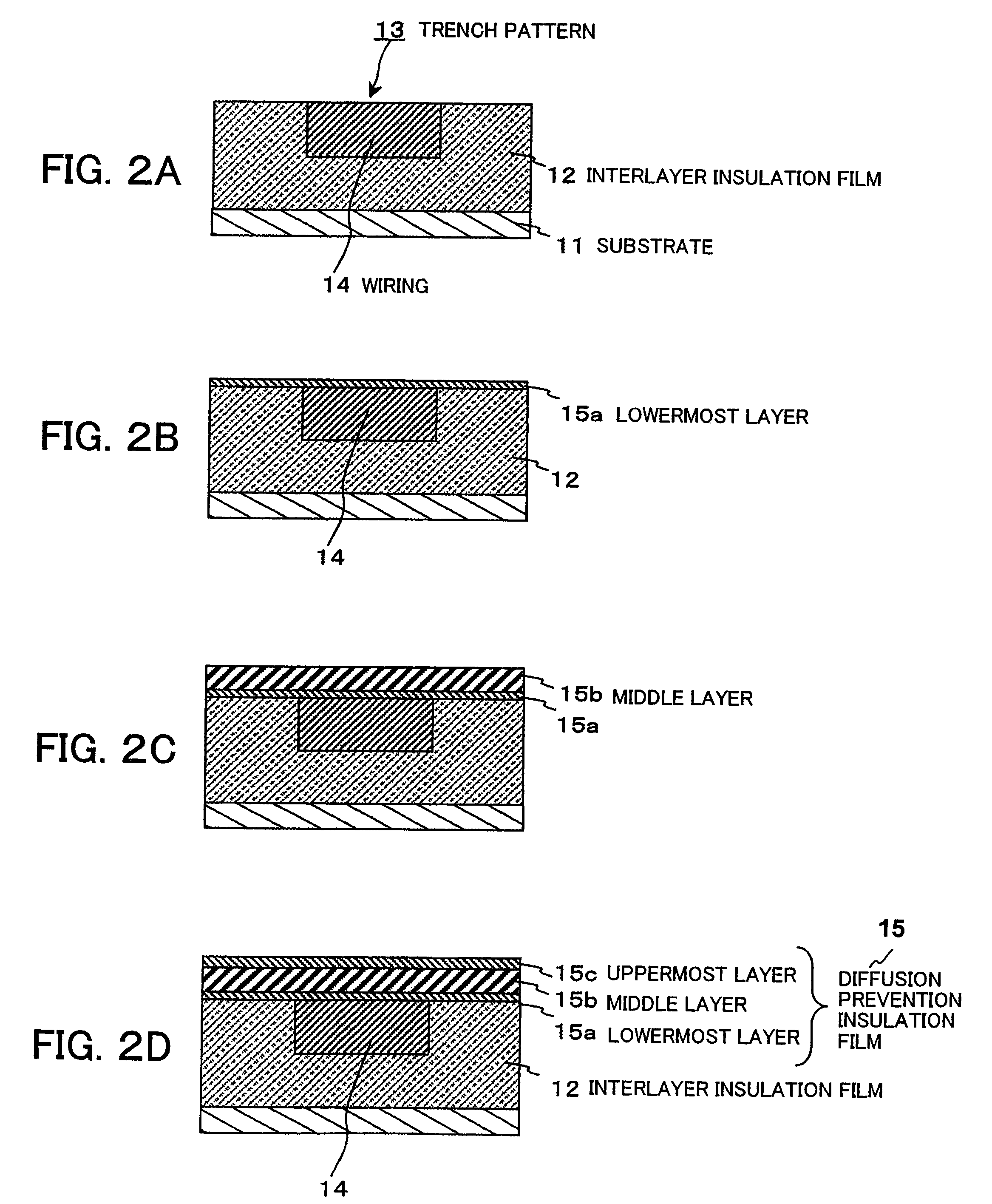
[0047]In the present example, an effect of preventing water permeation of the uppermost layer 15c in the diffusion prevention insulation film 15 of the semiconductor device explained in the embodiment shown in FIG. 1 was tested.

[0048]First, after forming a highly hygroscopic tetraethoxy silane (TEOS) film on a silicon (Si) substrate, a SiC film with low film density having a relative dielectric constant of 3.5 was formed on the TEOS film. The SiC film corresponds to the middle layer 15b in the diffusion prevention insulation film 15 of the present embodiment. After that, a SiCN film with high film density having a relative dielectric constant of 4.9 was formed to be a thickness of 5 nm on the SiC film. The SiCN film corresponds to the uppermost layer 15c in the diffusion prevention insulation film 15 of the present embodiment. The result was called a sample 1. On the other hand, what obtained by forming a TEOS film on a Si substrate, then, forming a SiC film having a relative dielec...

example 2

[0052]In the present example, the EM resistance of the diffusion prevention insulation film 15 in the semiconductor device explained in the embodiment was tested.

[0053]First, as shown in FIG. 1, a diffusion prevention insulation film 15 having the same configuration as that in the embodiment was formed in the same wiring structure as that in the embodiment. Specifically, the lowermost layer 15a and the uppermost layer 15c in the diffusion prevention insulation film 15 were SiCN films having a thickness of 5 nm, a relative dielectric constant of 4.9 and high film density, and the middle layer 15b was a SiC film with low film density having a relative dielectric constant of 3.5. The result is called a sample “A”. Also, what using a SiC film having a relative dielectric constant of 3.5 corresponding to the middle layer 15b of the present embodiment as a diffusion prevention insulation film 15 is called a sample “B”, and what using a SiC film having a relative dielectric constant of 3.8...


PUM


Abstract

A semiconductor device, wherein an increase of a capacity between wiring layers is suppressed, reliability of wiring and property of withstand voltage of a diffusion prevention insulation film can be improved and the wiring resistance can be maintained low, is provided by comprising an interlayer insulation film formed on a substrate, a wiring formed on a trench pattern formed on the interlayer insulation film, and a diffusion prevention insulation film formed on an upper surfaces of the interlayer insulation film including the wiring and preventing diffusion of metal from the wiring; wherein the diffusion prevention insulation film has a middle layer between a lowermost layer and an uppermost layer, wherein the lowermost layer is formed so as to contact the upper surfaces of the interlayer insulation layer including the wiring, the uppermost layer constitutes an uppermost portion of the diffusion prevention insulation film, and the middle layer has a lower relative dielectric constant than those of the lowermost layer and the uppermost layer.

Description

CROSS REFERENCES TO RELATED APPLICATIONS[0001]The present invention contains subject matter related to Japanese Patent Application JP 2004-147196 filed in the Japanese Patent Office on 18 May 2004, the entire contents of which being incorporated herein by reference.BACKGROUND OF THE INVENTION[0002]1. Field of the Invention[0003]The present invention relates to a semiconductor device, and particularly relates to a semiconductor device having a multilayer wiring structure using Cu wiring.[0004]2. Description of the Related Art[0005]In recent years, a technique on a wiring process has become increasingly significant for high-speed operating semiconductor integrated circuit devices (LSIs) as the LSIs become highly integrated. This is because disadvantages of a signal transmission delay have become noticeable as semiconductor elements become finer. To suppress an increase of the signal transmission delay, lower resistance of wiring, and a reduction of a capacity between wirings and a cap...

Claims


Application Information

Patent Timeline
Patent Type & Authority Patents(United States)
IPC IPC(8): H01L23/48H01L21/768H01L23/522H01L23/532
CPCH01L23/5222H01L23/53295H01L2924/0002H01L2924/00
Inventor TABUCHI, KIYOTAKAMIYAJIMA, HIDESHIMASUDA, HIDEAKI
Owner SONY CORP
Why Eureka
Try Eureka