Optimizing designing apparatus of integrated circuit, optimizing designing method of integrated circuit, and storing medium in which program for carrying out optimizing designing method of integrated circuit is stored

a technology of integrated circuits and designing apparatuses, applied in the field of optimizing designing apparatus of integrated circuits, optimizing designing methods of integrated circuits, and storing media, can solve the problems of inability to obtain designer requirements, inability to optimize circuit characteristics, and time-consuming optimization of circuits, so as to facilitate global optimization, facilitate optimization, and facilitate optimization

Active Publication Date: 2006-12-26
ABLIC INC
View PDF1 Cites 195 Cited by
  • Summary
  • Abstract
  • Description
  • Claims
  • Application Information

AI Technical Summary

Benefits of technology

[0035]The optimizing designing apparatus of the integrated circuit of the first aspect of the invention comprises the operation region judging means for judging the operation region (linear region, saturation region), the operation region analysis means for displaying the linear characteristics (Ids-Vgs characteristics) and saturation characteristics (Ids-Vds characteristics), and the SWEEP sensitivity analysis means for displaying the variation in output characteristics of the circuit. Since theses circuit analyses can be carried out, it is possible to easily carry out the LOCAL optimization and GLOBAL optimization, and a general circuit can be designed without special know-how.
[0051]The storing medium of the seventeenth aspect of the invention which stores the program for carrying out the optimizing designing method of the integrated circuit, the program displays variation in output characteristics of the circuit when the circuit parameter (gate width W, gate length L) is varied by ±α(%). Thus, it is possible to easily carry out the optimization.

Problems solved by technology

Any of them can optimize the circuit parameter (gate width and gate length) of a single transistor in the circuit, but there is a problem that the circuit characteristics can not be optimized only by optimizing the single transistor.
On the other hand, it is possible to optimize the entire circuit by improving an optimizing algorithm, but if the circuit parameter (gate width and gate length) of the single transistor is not optimized, there is a problem that it takes time to optimize the circuit or a result that a designer requires can not be obtained.
Therefore, there are problems that a portion which must be adjusted is generated other than a portion which was converted into a variable due to difference of transistor characteristics, that topology of the original integrated circuit can not be changed, that although simulation for optimization requires great time and this is not practical, a good result can not be obtained, that a result of an appropriate circuit parameter can not be obtained, that since a halfway result must be left when the procedure was suspended halfway while the optimization was being carried out, the optimization must be carried out from the beginning when the optimization is again carried out, that kinds of target performance in the optimization are limited, that there are too many parameters to be set and the operability is poor, that since the optimization is totally carried out automatically, a designer can not be involved in the operation during the optimization, that since the procedure and steps of the optimization are determined for every circuit model, there are many unnecessary optimization procedures, and that the procedure and steps of the optimization can not be saved for every circuit.

Method used


Image

  • Optimizing designing apparatus of integrated circuit, optimizing designing method of integrated circuit, and storing medium in which program for carrying out optimizing designing method of integrated circuit is stored
  • Optimizing designing apparatus of integrated circuit, optimizing designing method of integrated circuit, and storing medium in which program for carrying out optimizing designing method of integrated circuit is stored
  • Optimizing designing apparatus of integrated circuit, optimizing designing method of integrated circuit, and storing medium in which program for carrying out optimizing designing method of integrated circuit is stored

Examples


Embodiment Construction

[0064]An optimizing designing apparatus of an integrated circuit according to an embodiment of the present invention will be explained.

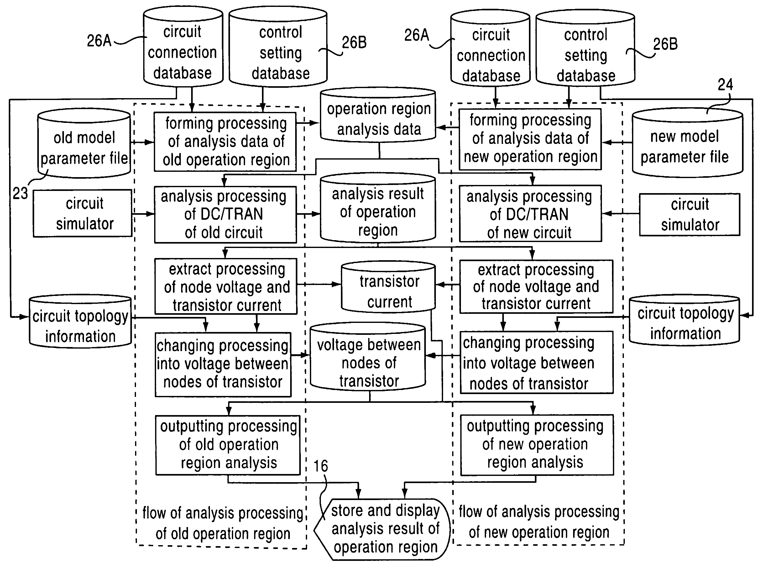
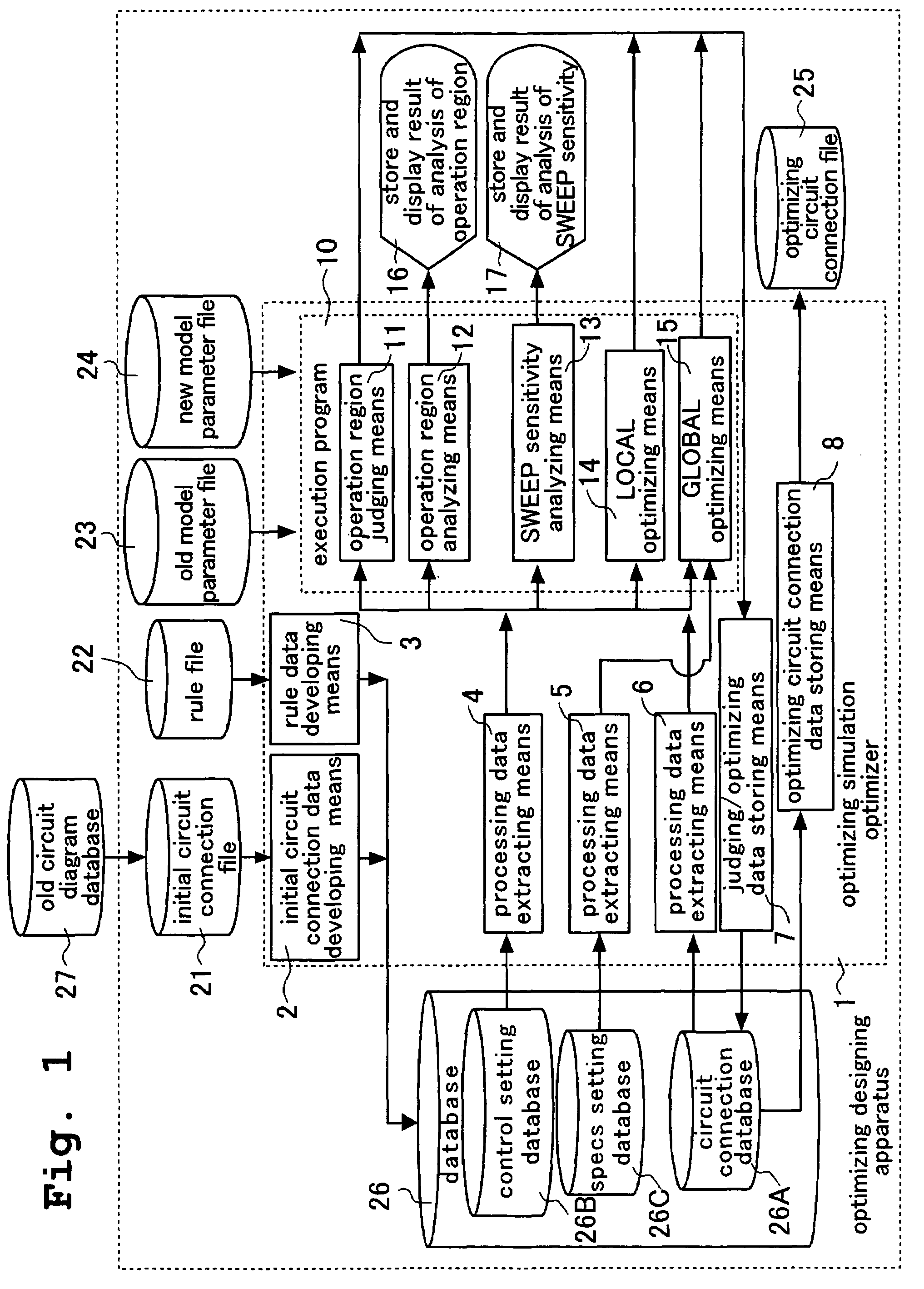
[0065]FIG. 1 is a block diagram showing the entire configuration of the optimizing designing apparatus of the integrated circuit according to the embodiment.

[0066]The optimizing designing apparatus of the integrated circuit according to the embodiment designs an optimizing circuit (second circuit) which is a new circuit having the same function as that of an initial circuit (first circuit) which is an old circuit when producing process or physical specification of a semiconductor is changed. The optimizing designing apparatus includes an optimizing simulation optimizer 1 which is an optimizing designing program and data storing means.

[0067]The data storing means comprises an initial circuit connection file 21, a rule file 22, an old model (first circuit) parameter file 23, a new model (second circuit) parameter file 24, an optimizing circuit (second ...


PUM


Abstract

It is an object of the present invention to provide a method, an apparatus and a program having high optimization precision and capable of obtaining an answer required by a designer in a short time by combining optimization between individual transistors and optimization as the entire circuit, or by appropriately combining judgment of an operation region, an analysis of the operation region and a SWEEP sensitivity analysis when the optimization is carried out. An optimizing designing apparatus of an integrated circuit for designing a circuit, comprises operation region judging means for adjusting an operation region (linear region, saturation region) of the circuit, operation region analysis means for displaying liner characteristics (Ids-Vgs characteristics) of the circuit and saturation characteristics (Ids-Vds characteristics) of the circuit, and SWEEP sensitivity analysis means for displaying variation in output characteristics of the circuit.

Description

TECHNICAL FIELD[0001]The present invention relates to an optimizing designing apparatus of an integrated circuit and an optimizing designing method of the integrated circuit which designs a second circuit having the same function and performance as those of a first circuit when a producing process or a physical specification of semiconductor is changed. The invention also relates to a storing medium in which a program for carrying out the optimizing designing method of the integrated circuit is stored.BACKGROUND TECHNIQUE[0002]In a patent document 1 as a conventional technique, an operation of a circuit is simulated, and a parameter of the circuit (gate width and gate length) is optimized based on information of difference between the simulated value and a target value, thereby optimizing the operation of the circuit.[0003]In patent documents 2 and 3, a parameter (gate width and gate length) of a circuit is optimized based on operation point characteristics of a MOS transistor of a ...

Claims


Application Information

Patent Timeline
Patent Type & Authority Patents(United States)
IPC IPC(8): G06F17/50H01L21/82H03K19/00
CPCG06F17/5036G06F17/5045G06F30/30G06F30/367
Inventor MORI, KENJINAKAJIMA, TAKASHI
Owner ABLIC INC
Why Eureka
Try Eureka