
Electrical contacting method

a contact method and electric technology, applied in the direction of electrical equipment, climate sustainability, printed circuit aspects, etc., can solve the problems of wasting and achieve the effects of improving contact reliability, extreme mechanical stability, and saving space on the circuit board

Active Publication Date: 2007-01-02
NOVAR PLC
View PDF13 Cites 17 Cited by
  • Summary
  • Abstract
  • Description
  • Claims
  • Application Information

AI Technical Summary

Benefits of technology

[0007]An important aspect of the present invention is therefore to extend the printed conductors to be contacted on the panel, i.e., the sheet from which the circuit board(s) subsequently will be isolated, over the eventual edge of the circuit board(s) in the same raster in which the printed conductors of the MID component end at this edge, provide these printed conductors with plated-through through holes precisely at the height of the eventual edge, and only then break or stamp the circuit boards out of the panel, for example, so that each printed conductor ends at a metal-plated semi-cylindrical surface. In the case of a single board, it is sufficient if the panel is larger than the circuit board by an appropriate edge strip. This edge strip is provided with the through holes made into through contacts at the height of the eventual, actual edge of the board. The excess edge strips are subsequently broken off. If, as is typical, multiple circuit boards are to be produced simultaneously, it is significantly more favorable to proceed according to the above-mentioned option of having multiple circuit boards formed on the panel. At least two circuit boards then lie head-to-head in relation to one another on the panel, e.g., in such a way that the layout of one circuit board is produced on the panel rotated by 180° around the vertical axis in relation to the other circuit board. A printed conductor raster is expediently produced over essentially the entire length of the relevant edge, independently of how many printed conductors conduct electric signals. This is also true for the corresponding edge of the MID component. In this way, the maximum strength is achieved for the mechanical connection between the circuit board and the MID component.
[0012]The mechanical strength is favorable above all if the circuit board and the MID component are positioned in relation to one another so that the printed conductors of the circuit board and of the MID component to be contacted with one another are offset from one another in height by approximately the thickness of the circuit board and overlap. In this way, a soldered connection with a larger area is provided between the circuit board and the MID component.

Problems solved by technology

Simultaneously, it also saves space on the circuit board and dispenses with the additional manufacturing steps which the contacting methods previously known from the related art required.

Method used


Image

  • Electrical contacting method
  • Electrical contacting method
  • Electrical contacting method

Examples


Embodiment Construction

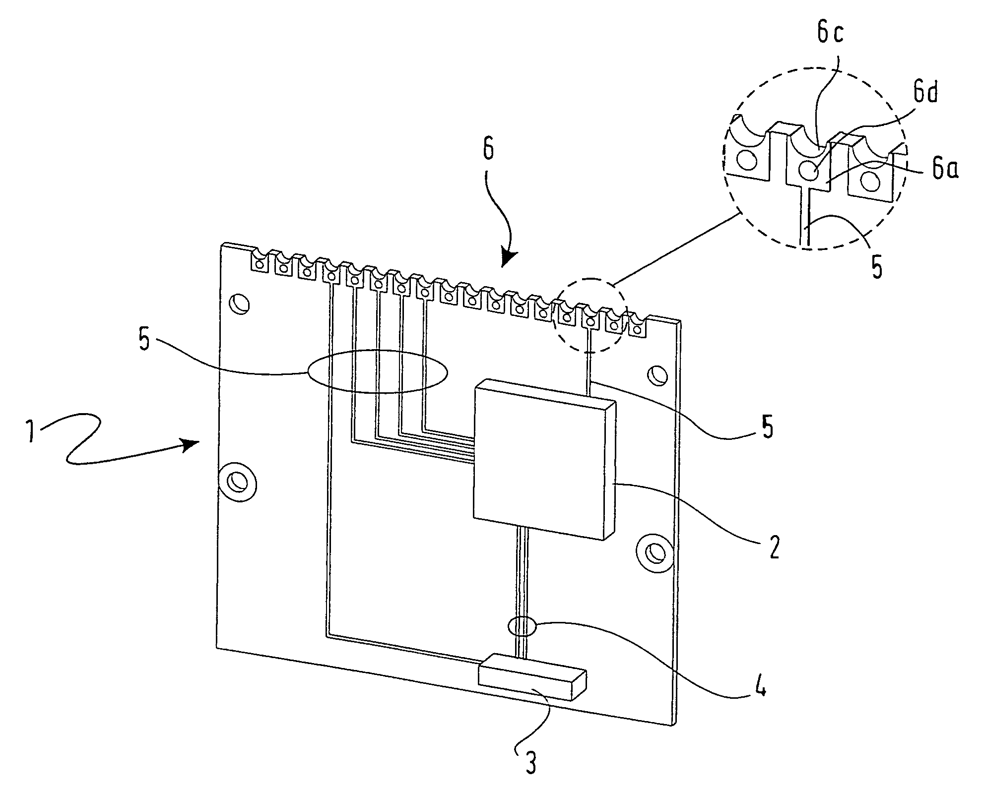
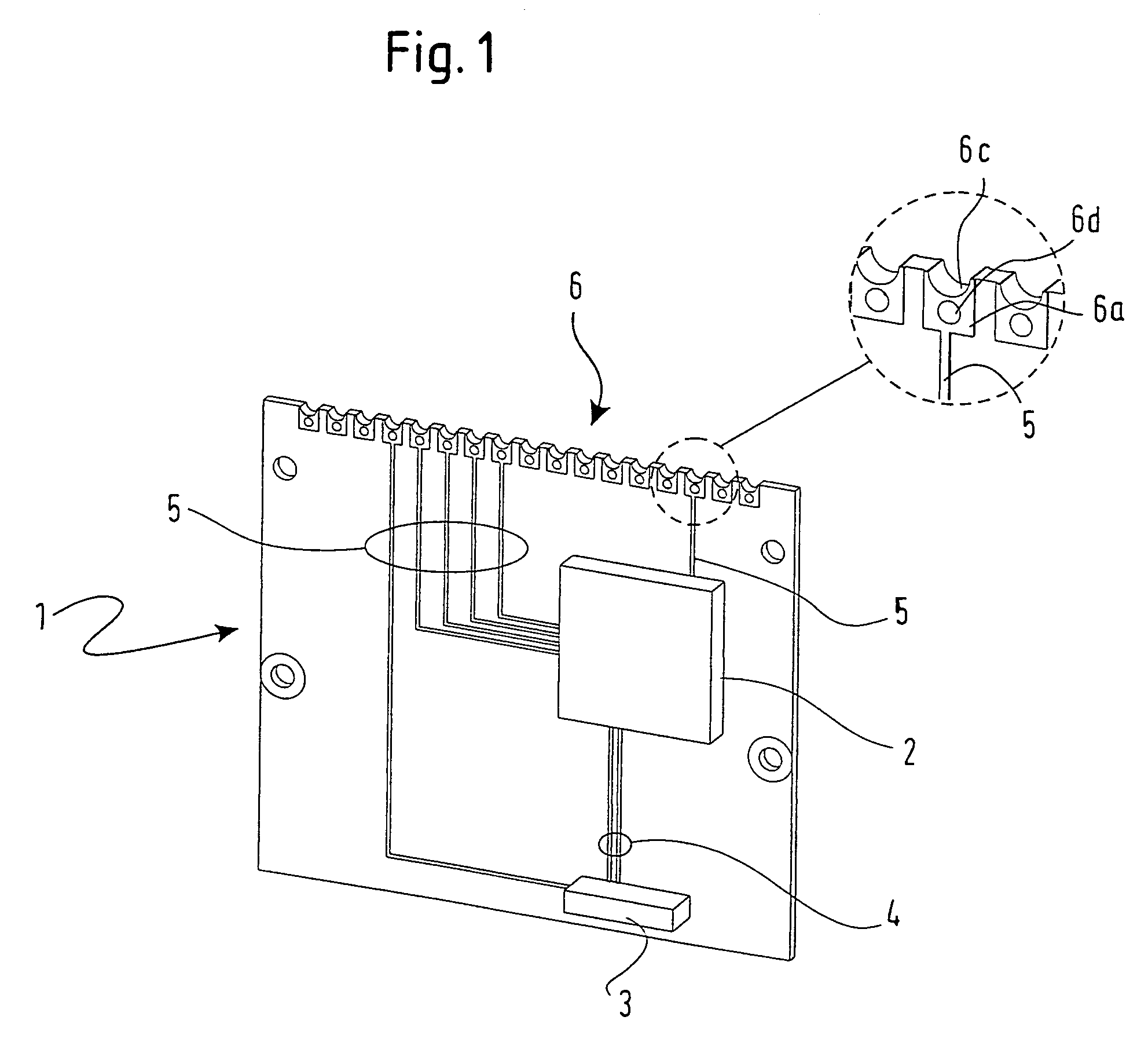
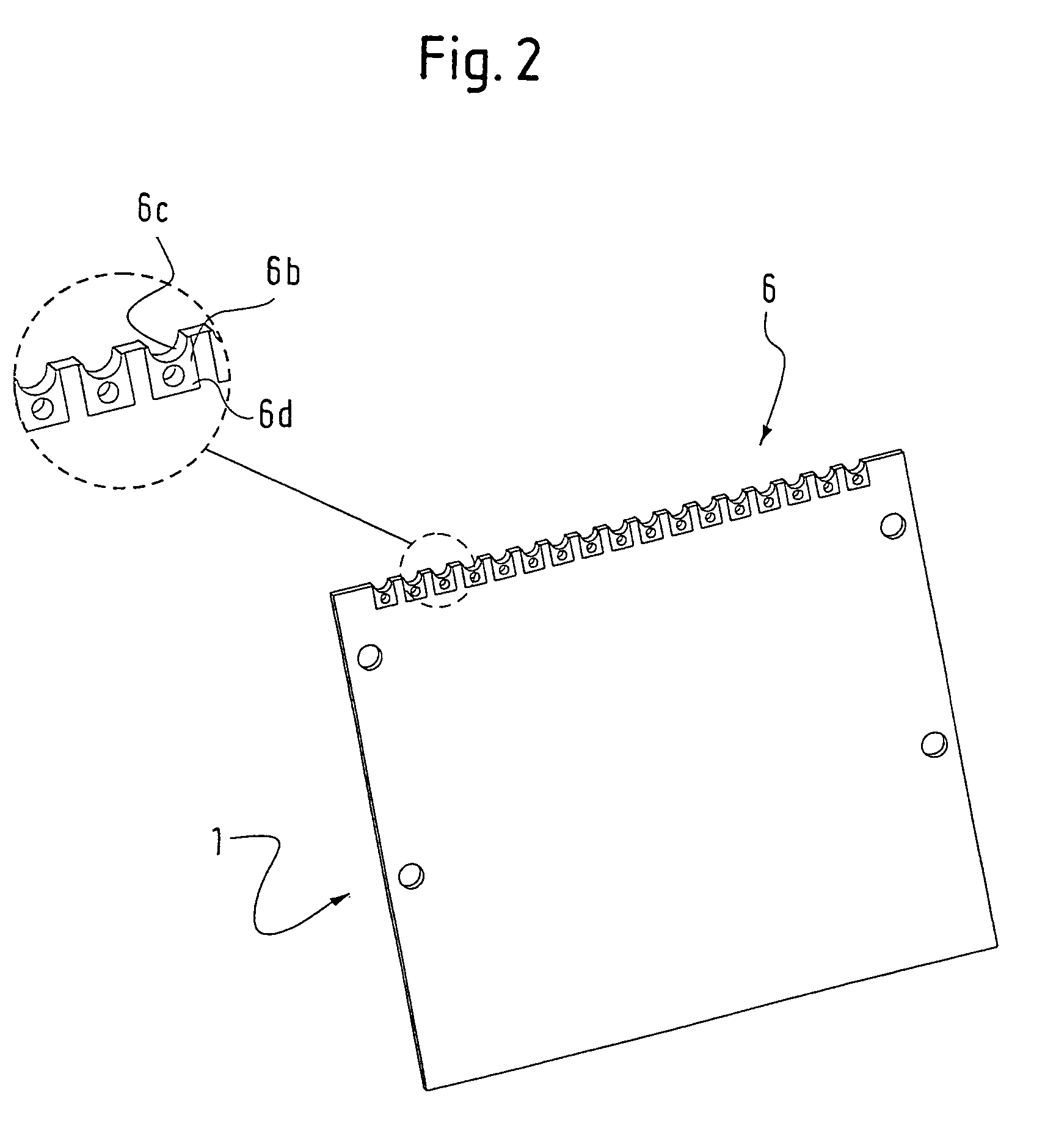
[0023]FIG. 1 shows a simplified perspective view of a circuit board 1 which is made of fiberglass-reinforced epoxide resin for example and which is equipped with components 2 and 3 (shown only symbolically in FIG. 1), which are connected to one another via printed conductors 4. Power supply and signal terminals of the components 2 and 3 extend to edge contacts 6 at the upper edge of the circuit board via further printed conductors 5. There, each printed conductor passes into widened contacting area 6a (cf. the enlarged detail in FIG. 1). The contacting areas 6a are positioned in a predetermined raster, along nearly the entire upper edge of the circuit board 1, even if the contacting areas are not necessary as extended electrical terminals. The circuit board 1 may also be provided with printed conductors and equipped with electrical components on its back.

[0024]Even if the circuit board is provided with printed conductors and components only on the front, as shown in this exemplary e...


PUM

PropertyMeasurementUnit
Thicknessaaaaaaaaaa
Areaaaaaaaaaaa

Abstract

A method for contacting printed conductors terminating at the edge of a circuit board with printed conductors of a MID component includes: on a panel which includes the circuit board, producing the printed conductors of the circuit board in a layout in which the printed conductors are extended past a partition line which defines the edge of the circuit board; providing the panel with through holes along the partition line in the region of the printed conductors; electroplating through the through holes; isolating the circuit board from the panel; and positioning the circuit board in relation to the MID component and soldering the printed conductors of the circuit board to the printed conductors of the MID component. Rear electrical contacting areas are provided on a back side of the panel near the partition line, and the printed conductors are connected to the rear electrical contacting areas via the through holes.

Description

CROSS REFERENCE TO RELATED APPLICATIONS[0001]This application claims priority under 35 U.S.C. §119(e) to German Application No. DE 10325550.8, filed on Jun. 5, 2003, and titled “Electrical Contacting Method,” the entire contents of which are hereby incorporated by reference.FIELD OF THE INVENTION[0002]The present invention relates to a method for electrically contacting printed conductors terminating on at least one edge of a circuit board with printed conductors located on an adjoining component made of a thermoplastic in MID technology.BACKGROUND[0003]Electrical components may be provided as molded injection devices (MID) with desired printed conductors, i.e., when manufactured in MID technology, using different methods, e.g., a masking method, in two-component injection molding with subsequent electroplating, through laser direct structuring, through coating the back of a film, or through hot stamping. In contrast to conventional circuit boards made of fiberglass-reinforced plast...

Claims


Application Information

Patent Timeline
IPC IPC(8): H05K3/34H05K1/00H05K3/00H05K3/36H05K3/40H05K3/42
CPCH05K3/3442H05K3/403H05K1/0284Y10T29/49165H05K3/3405H05K3/368H05K3/42H05K2201/09118H05K2201/09181H05K2201/09481H05K2201/10666H05K2203/0455Y10T29/49117Y10T29/49126Y10T29/49144Y10T29/49789H05K3/0052Y02P70/50
Inventor GERNHARDT, ANGELIKAGOULET, THOMASMENZEL, CARSTENOLLIK, WALDEMAR
Owner NOVAR PLC
Learn More