Method for fabrication of semiconductor device

a semiconductor laser and fabrication method technology, applied in the direction of semiconductor lasers, lasers, semiconductor laser structural details, etc., can solve the problems of low yield, difficult to further divide the bar into discrete nitride semiconductor laser devices, and low yield, so as to prevent crack development and good surface flatness

Inactive Publication Date: 2007-01-02
SHARP KK
View PDF15 Cites 26 Cited by
  • Summary
  • Abstract
  • Description
  • Claims
  • Application Information

AI Technical Summary

Benefits of technology

[0032]In view of the conventionally encountered problems discussed above, it is an object of the present invention to provide a semiconductor device and a method for the fabrication thereof wherein development of cracks is prevented when a semiconductor device such as a nitride semiconductor laser device is produced by laying a nitride semiconductor growth layer on top of a substrate having a nitride semiconductor layer in at least part of the surface thereof and in addition wherein current leak paths and damage are eliminated by forming a nitride semiconductor growth layer having good surface flatness by suppressing formation of a nitride semiconductor thin film as a result of atoms and molecules of the source materials from which the nitride semiconductor thin film is formed migrating or otherwise moving from top growth portions on the surface of ridges into engraved regions.
[0069]With any of the above-described methods, it is possible to prevent the engraved region from being filled by the nitride semiconductor thin films, and to prevent different parts of the nitride semiconductor thin films from meeting above the engraved region and forming hollow spaces.

Problems solved by technology

One conventional problem with nitride semiconductors is that, in the fabrication of nitride semiconductor devices as exemplified by nitride semiconductor laser devices, the yield, i.e., the ratio of the number of properly working nitride semiconductor laser devices to the total number of those produced on a single wafer, is extremely low.
However, since a nitride semiconductor substrate of a nitride semiconductor such as n-type GaN has a hexagonal crystal structure and thus does not have cleavage surfaces in the direction parallel to the direction of the resonators, it is difficult to split the bar further into discrete nitride semiconductor laser devices.
Thus, the splitting here causes chipping and cracking, and in addition cleavage in unintended directions, leading to a low yield.
Another cause for a low yield is development of cracks.
Here, the different films forming the nitride semiconductor growth layer have different lattice constants, and thus cause lattice mismatch, resulting in development of cracks.
Disappointingly, however, when nitride semiconductor laser devices were produced by the use of the technique disclosed in Japanese Patent Application Laid-Open No. 2002-246698 mentioned above, with an n-type GaN substrate used as a substrate 10 and with a nitride semiconductor growth layer 11 epitaxially grown on top of this n-type GaN substrate by MOCVD or the like, it was indeed possible to reduce cracks, but it was not possible to significantly increase the yield.
This large distribution of the layer thickness within the wafer surface is considered to result from the fact that the growth rate of the film that is epitaxially grown at the ridges on the processed substrate including a nitride semiconductor substrate varies under the influence of the engraved regions, resulting in uneven growth rates within the wafer surface.
Moreover, it has been found that, when nitride semiconductor laser devices are produced by the technique disclosed in Japanese Patent Application Laid-Open No. 2002-246698 mentioned above, if electrodes are formed in depressions on the surface of the nitride semiconductor growth layer 11, current leak paths develop in the depressions, making it impossible to obtain a normal I-V characteristic.
The presence of the depressions here, however, causes the insulating film to be formed unevenly on the surface, leaving a large number of small cracks, very thin regions, small holes (pits), and the like.
Thus, through unevenly formed parts of the insulating film, current leaks.
H5-315646 mentioned above are separated from one another, since it is after a nitride semiconductor growth layer is laid on top of the nitride semiconductor substrate that grooves are formed by the use of a dicing machine, the nitride semiconductor growth layer may be internally damaged, degrading the characteristics of the nitride semiconductor laser devices.

Method used


Image

  • Method for fabrication of semiconductor device
  • Method for fabrication of semiconductor device
  • Method for fabrication of semiconductor device

Examples


first embodiment

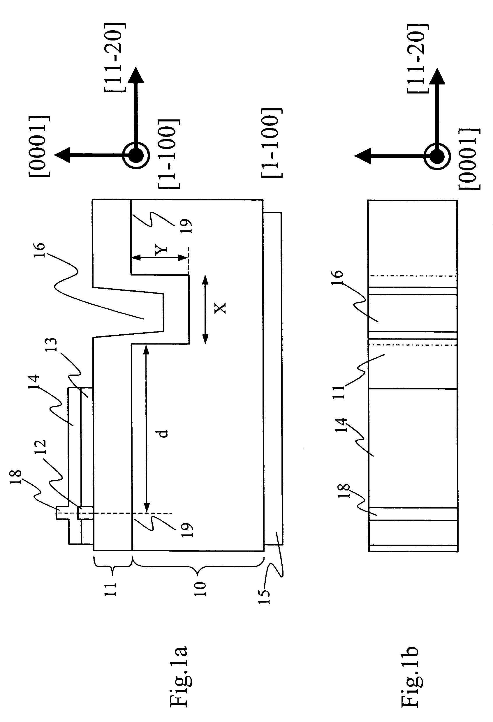
[0111]Now, a first embodiment of the present invention will be described with reference to the relevant drawings. This embodiment deals with, as an example of a nitride semiconductor device, a nitride semiconductor laser device. It should be understood, however, that the present invention is applicable to any other type of nitride semiconductor device. FIG. 1a is a schematic sectional view of the nitride semiconductor device of this embodiment, and FIG. 1b is a top view of FIG. 1a. FIG. 3b is a schematic sectional view of a processed substrate 10 before a nitride semiconductor thin film is grown thereon in this embodiment of the invention, and FIG. 3a is a top view of FIG. 3b. In these figures, plane orientations are indicated together. The nitride semiconductor laser device shown in FIGS. 1a and 1b is produced, for example, by laying, on top of the processed substrate 10 shown in FIGS. 3a and 3b, a nitride semiconductor growth layer 11 having a structure as shown in FIG. 19.

[0112]T...

second embodiment

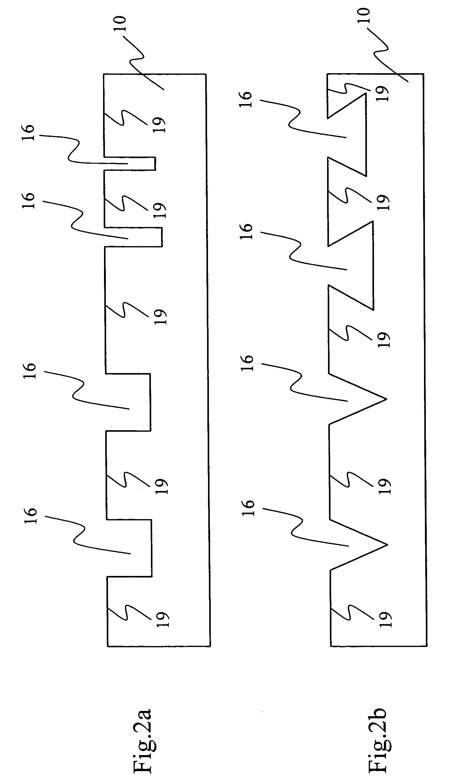
[0146]Next, a second embodiment of the present invention will be described with reference to the relevant drawings. This and the following embodiments both deal with, as an example of a semiconductor device, a nitride semiconductor laser device. It should be understood, however, that the present invention is applicable to any other type of semiconductor device. FIG. 11a is a schematic sectional view of the semiconductor device of this embodiment, and FIG. 11b is a top view of FIG. 11a. FIG. 12b is a schematic sectional view of a processed substrate 10 before a nitride semiconductor thin film is grown thereon in this embodiment of the invention, and FIG. 12a is a top view of FIG. 12b. In FIGS. 11a, 11b, 12a, and 12b, plane orientations are indicated together.

[0147]In the nitride semiconductor laser device of this embodiment, a processed substrate 10 formed of a nitride semiconductor substrate having engraved regions 16 formed as depressed portions thereon further has SiO2 walls forme...

third embodiment

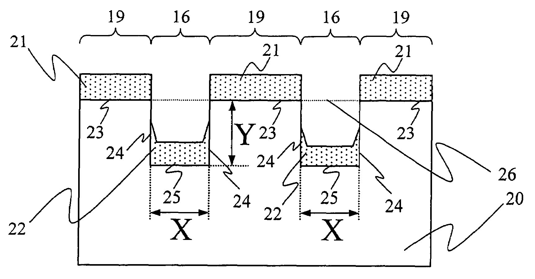
[0181]Next, a third embodiment of the present invention will be described with reference to the relevant drawings. FIG. 16 is a schematic sectional view of part of a wafer having nitride semiconductor thin films grown on top of a processed substrate 10 in this embodiment. In this embodiment, unlike in the second embodiment, no SiO2 walls are formed along the edges of ridges 19, i.e., the non-engraved regions, on the processed substrate 10.

[0182]FIG. 16 is a schematic sectional view of a wafer having nitride semiconductor thin films grown on such a processed substrate 10 having engraved regions 16 formed thereon. As shown in FIG. 16, the nitride semiconductor thin films grow as top growth portions 95 in central portions of top portions 91 of the ridges 19, as inflow prevention portions 94 in both edge portions of the top portions 91 of the ridges 19, near the engraved regions 16, and as engraved region growth portions 97 on side portions 92 and floor portions 93 in the engraved regio...


PUM

PropertyMeasurementUnit
widthaaaaaaaaaa
widthaaaaaaaaaa
opening widthaaaaaaaaaa

Abstract

On a processed substrate having an engraved region as a depressed portion formed thereon, a nitride semiconductor thin film is laid. The sectional area occupied by the nitride semiconductor thin film filling the depressed portion is 0.8 times the sectional area of the depressed portion or less.

Description

[0001]This nonprovisional application claims priority under 35 U.S.C. § 119(a) on Patent Applications Nos. 2004-139919 and 2004-172291 filed in Japan on May 10, 2004 and Jun. 10, 2004, respectively, the entire contents of which are hereby incorporated by reference.BACKGROUND OF THE INVENTION[0002]1. Field of the Invention[0003]The present invention relates to a semiconductor device such as a nitride semiconductor laser device, and to a method for the fabrication thereof.[0004]2. Description of Related Art[0005]As compared with AlGaInAs- and AlGaInP-based semiconductors, nitride semiconductors such as GaN, AlGaN, GaInN, AlGaInN, and mixed crystals thereof are characterized by their larger band gaps Eg and their being direct-transition semiconductor materials. These properties make nitride semiconductors attractive materials for semiconductor light-emitting devices such as semiconductor lasers that emit light in a short-wavelength region from ultraviolet to green and light-emitting di...

Claims


Application Information

Patent Timeline
Patent Type & Authority Patents(United States)
IPC IPC(8): H01L21/00H01L33/20H01L33/24H01L33/32H01S5/02H01S5/22H01S5/223H01S5/323
CPCH01S5/2231H01S5/32341H01L33/20H01L33/24H01L33/32H01S5/0202H01S2304/12H01S5/2201H01S5/0207
Inventor KAMIKAWA, TAKESHIYAMADA, EIJIARAKI, MASAHIRO
Owner SHARP KK
Why Eureka
Try Eureka