Switched capacitor input circuit and method therefor

a technology of input circuit and input buffer, which is applied in the field of electrical circuits, can solve the problems of poor noise performance of design, no longer linear relationship of output voltage to input voltage, and poor linearity of known input buffers

Inactive Publication Date: 2007-01-02
SILICON LAB INC
View PDF10 Cites 33 Cited by
  • Summary
  • Abstract
  • Description
  • Claims
  • Application Information

AI Technical Summary

Problems solved by technology

Known input buffers suffer from poor linearity when the input range is a significant fraction of the power supply voltage.
The unity-gain follower suffers from the drawback that when the input voltage is close the power supply voltage rails, the current source transistors in the amplifier start to come out of saturation, causing the output voltage to no longer be linearly related to the input voltage.
This design has poor noise performance because the system noise will be amplified by the attenuation ratio.
The bandwidth requirement is difficult to maintain when low current consumption is required.
Furthermore this design cannot recognize signals that are close to ground.

Method used


Image

  • Switched capacitor input circuit and method therefor
  • Switched capacitor input circuit and method therefor
  • Switched capacitor input circuit and method therefor

Examples


Embodiment Construction

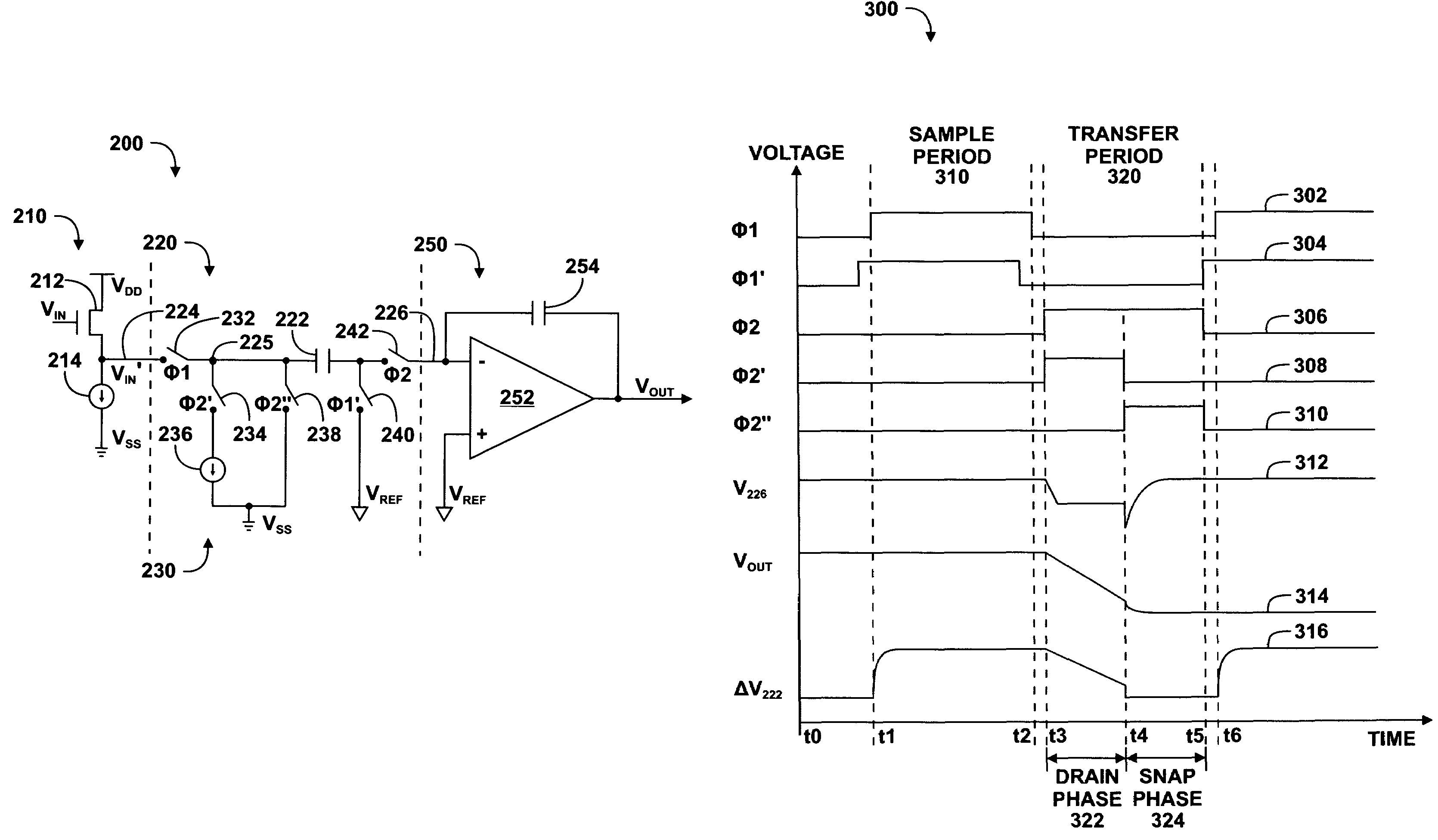
[0022]The following detailed description is merely exemplary in nature and is not intended to limit the invention or the application and uses of the invention. Furthermore, there is no intention to be bound by any expressed or implied theory presented in the preceding technical field, background, brief summary or the following detailed description.

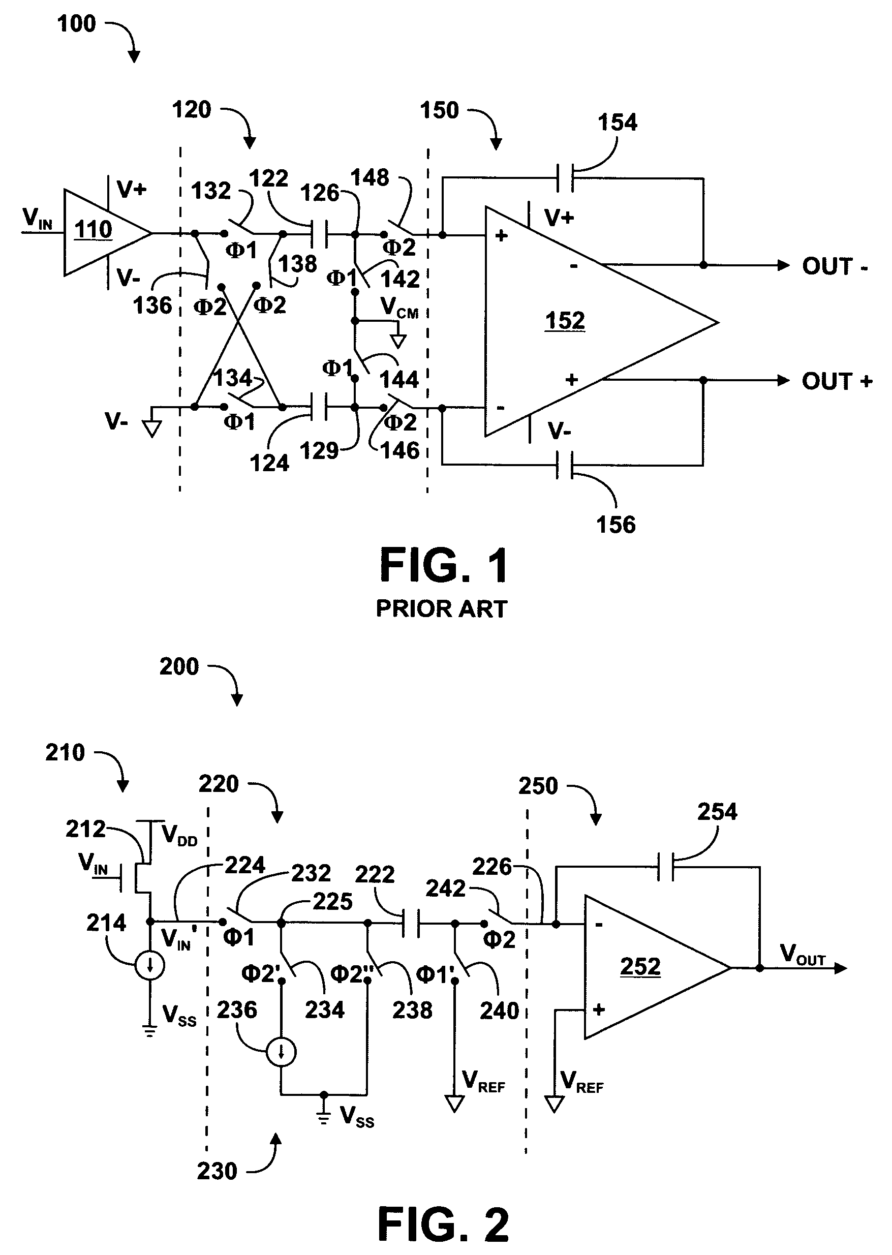
[0023]FIG. 1 illustrates in partial block diagram and partial schematic form a switched capacitor input circuit 100 known in the prior art. Switched capacitor input circuit 100 includes generally an input buffer 110, a switched capacitor sampler circuit 120, and an integrator 150. Input buffer 110 has an input terminal for receiving an input voltage labeled “VIN”, and an output terminal, and is powered from a positive power supply voltage terminal (“rail”) labeled “V+” and a negative power supply voltage rail labeled “V−”.

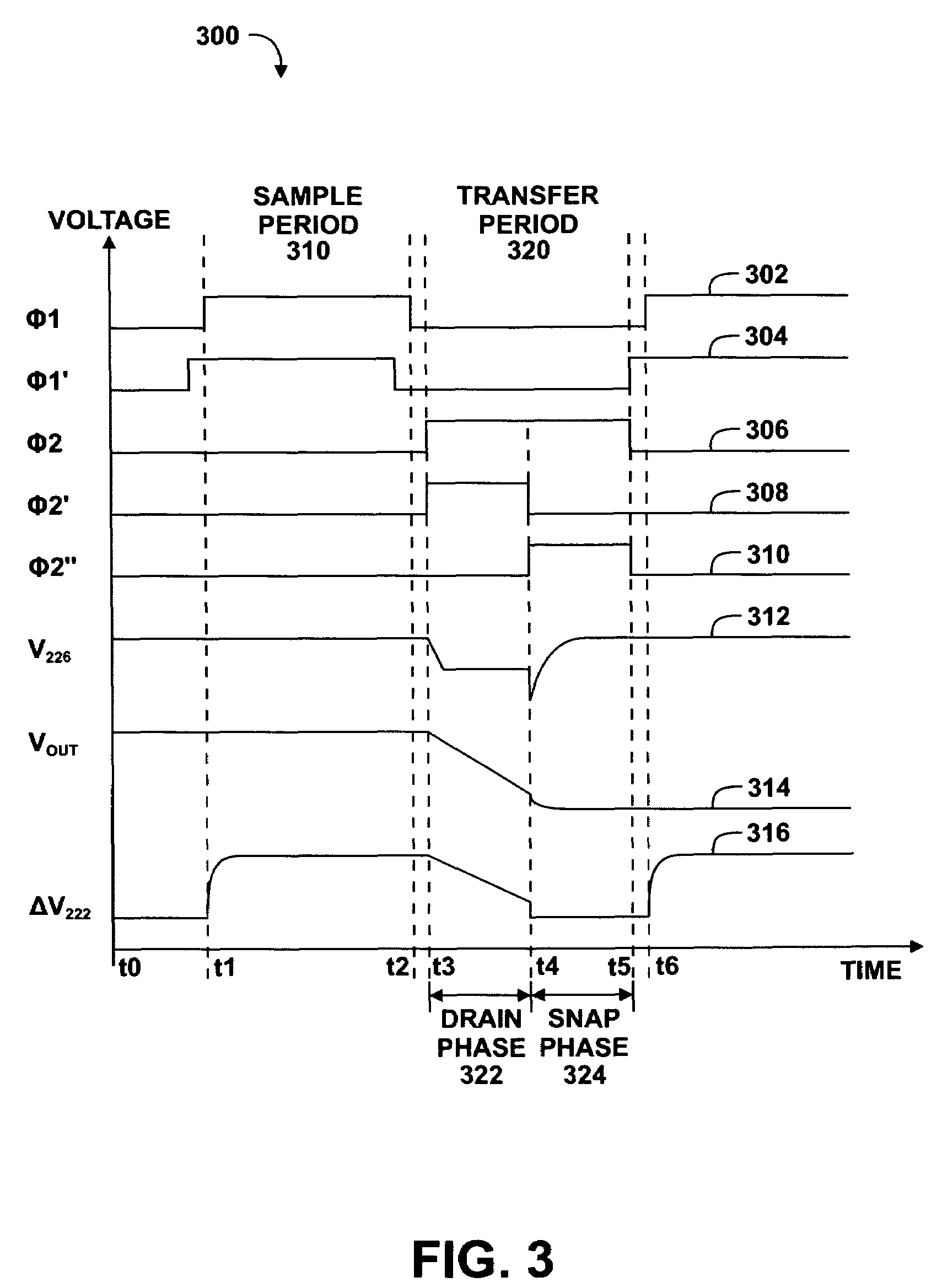
[0024]Switched capacitor sampler circuit 120 includes a capacitor 122, a capacitor 124, and switches 132, 134, 136, 138...


PUM


Abstract

A switched capacitor input circuit (200) includes an input buffer (210), a switched capacitor sampler circuit (220), and an integrator (250). The input buffer (210) has an input terminal for receiving an input voltage, and an output terminal. The switched capacitor sampler circuit (220) has an input terminal coupled to the output terminal of the input buffer (210), and an output terminal. The switched capacitor sampler circuit (220) includes a capacitor (222) and stores a charge proportional a voltage at the output terminal of the input buffer (210) in the capacitor (222) during a sample period, and transfers the charge from the capacitor (222) to the output terminal thereof during a transfer period subsequent to the sample period in a plurality of charge portions corresponding to a like plurality of phases of the transfer period. The integrator (250) has an input terminal coupled to the output terminal of the switched capacitor sampler circuit, and an output terminal for providing an output voltage signal.

Description

CROSS REFERENCE TO RELATED, COPENDING APPLICATION[0001]Related subject matter is found in a copending patent application entitled “Switched Capacitor Sampler Circuit and Method Therefor,” application Ser. No. 11 / 003,288, invented by Derrick Chunkai Wei, filed of even date herewith and assigned to the assignee hereof.TECHNICAL FIELD[0002]The present application generally relates to electrical circuits, and more particularly to switched capacitor circuits and input buffers using such switched capacitor circuits.BACKGROUND[0003]A phase locked loop (PLL) is a circuit that can be used to generate an output clock signal at a selectable output frequency from a reference clock signal at a lower frequency. A classical PLL includes a phase detector that detects a difference in phase between a reference clock signal and a divided down version of the output clock signal. The output clock signal is generated by a voltage controlled oscillator (VCO). The output of the phase detector is used to ad...

Claims


Application Information

Patent Timeline
Patent Type & Authority Patents(United States)
IPC IPC(8): G06G7/19
CPCH03F3/005
Inventor WEI, DERRICK CHUNKAI
Owner SILICON LAB INC
Why Eureka
Try Eureka