Integrated code and data flash memory

a code and data flash technology, applied in the field of integrated circuits, can solve the problems of high design difficulty, low system space on the board, and inability to integrate conventional flash memory technology for both code and data flash purposes, and achieve the effects of low cost, high yield and easy manufacturing

Active Publication Date: 2007-01-02
MACRONIX INT CO LTD
View PDF39 Cites 118 Cited by
  • Summary
  • Abstract
  • Description
  • Claims
  • Application Information

AI Technical Summary

Benefits of technology

[0009]The present invention provides a memory architecture for an integrated circuit, a method for manufacturing an integrated circuit, and a method for operating an integrated circuit, where the integrated circuit comprises a first memory array configured to store data for one pattern of data usage and a second memory array configured to store data for another pattern of data usage. The first and second memory arrays comprise nonvolatile memory cells, and more preferably charge storage based nonvolatile memory cells. A first operation algorithm adapted in preferred embodiments for data flash applications is used for programming, erasing and reading data in the first memory array. A second operation algorithm adapted in preferred embodiments for code flash applications is used for programming, erasing and reading data in the second memory array, wherein the second operation algorithm is different than the first operation algorithm. In some embodiments of the invention, the memory cells in the first and second arrays have substantially the same structure, so that one die with memory for both code flash and data flash applications can be easily manufactured using a simple process, at low cost and high yield.
[0010]According to embodiments of the present invention, the nonvolatile memory cells in at least one of the first and second memory arrays, and in more preferred embodiments in both of the first and second memory arrays, comprise a first channel terminal acting as a source or drain, a channel and a second channel terminal acting as a drain or source in the semiconductor substrate. A charge storage structure overlies the channel, and typically part of the first and second channel terminals. The charge storage structure in some embodiments comprises a first dielectric layer, a localized charge trapping structure such as a layer of silicon nitride, and a second dielectric layer. In one particular embodiment, the first dielectric layer acts as a tunnel dielectric adapted for both the first and second operation algorithms. In another embodiment, the first and the second dielectric layers are configured as tunnel dielectrics. For example, the tunnel dielectric in one embodiment comprises silicon dioxide or silicon oxynitride having a thickness supporting band-to-band tunneling induced hole injection and channel hot electron injection, and the second dielectric is configured with a thickness supporting E-field assisted (Fowler-Nordheim) tunneling from the gate to the charge trapping structure. In the other embodiments, one or both of the first and the second dielectric layers are configured as charge blocking dielectrics. For example, the blocking dielectric in one embodiment comprises silicon dioxide or silicon oxynitride having a thickness to prevent the stored charges in the charge trapping layer from escaping out during storage period, which can improve data retention. Other types of nonvolatile memory cell structures, including for example floating gate type cells and localized charge trapping type cells, may be used in other embodiments of the invention.
[0014]Yet another aspect of the present invention provides a method for storing data for data flash applications and data for code flash applications on a single integrated circuit. According to an embodiment of the invention, the method comprises addressing a first memory array comprising nonvolatile memory cells on the integrated circuit to read, program and erase data using a first operation algorithm, and addressing a second memory array comprising nonvolatile memory cells on the integrated circuit to read, program and erase data according to a second operation algorithm. In embodiments of the invention, the nonvolatile memory cells in the first and second memory arrays have substantially the same structure. The first and second operation algorithms differ from one another, so that the first and second memory arrays may be more efficiently utilized for different patterns of data usage. As described above, the first and second operation algorithms are adapted in a preferred embodiment for data flash applications and code flash applications respectively.

Problems solved by technology

Thus, integration of conventional flash memory technology for both code and data flash purposes on a single chip has not been practical.
The cost of systems in terms of space on the board, the number of chips, and difficulty in design is high as a result.

Method used


Image

  • Integrated code and data flash memory
  • Integrated code and data flash memory
  • Integrated code and data flash memory

Examples


Embodiment Construction

[0025]A detailed description of embodiments of the present invention is provided with reference to FIGS. 1–7.

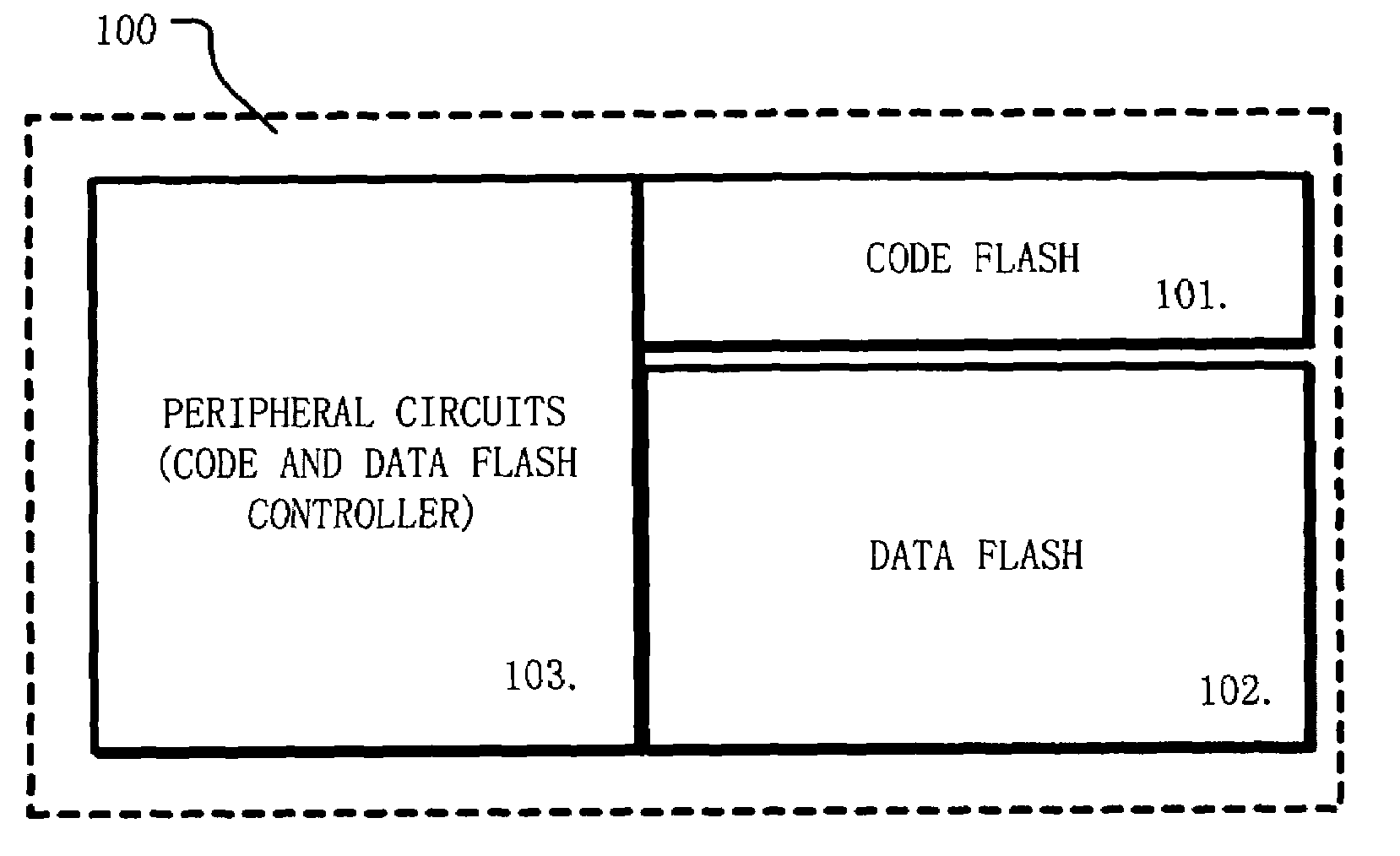
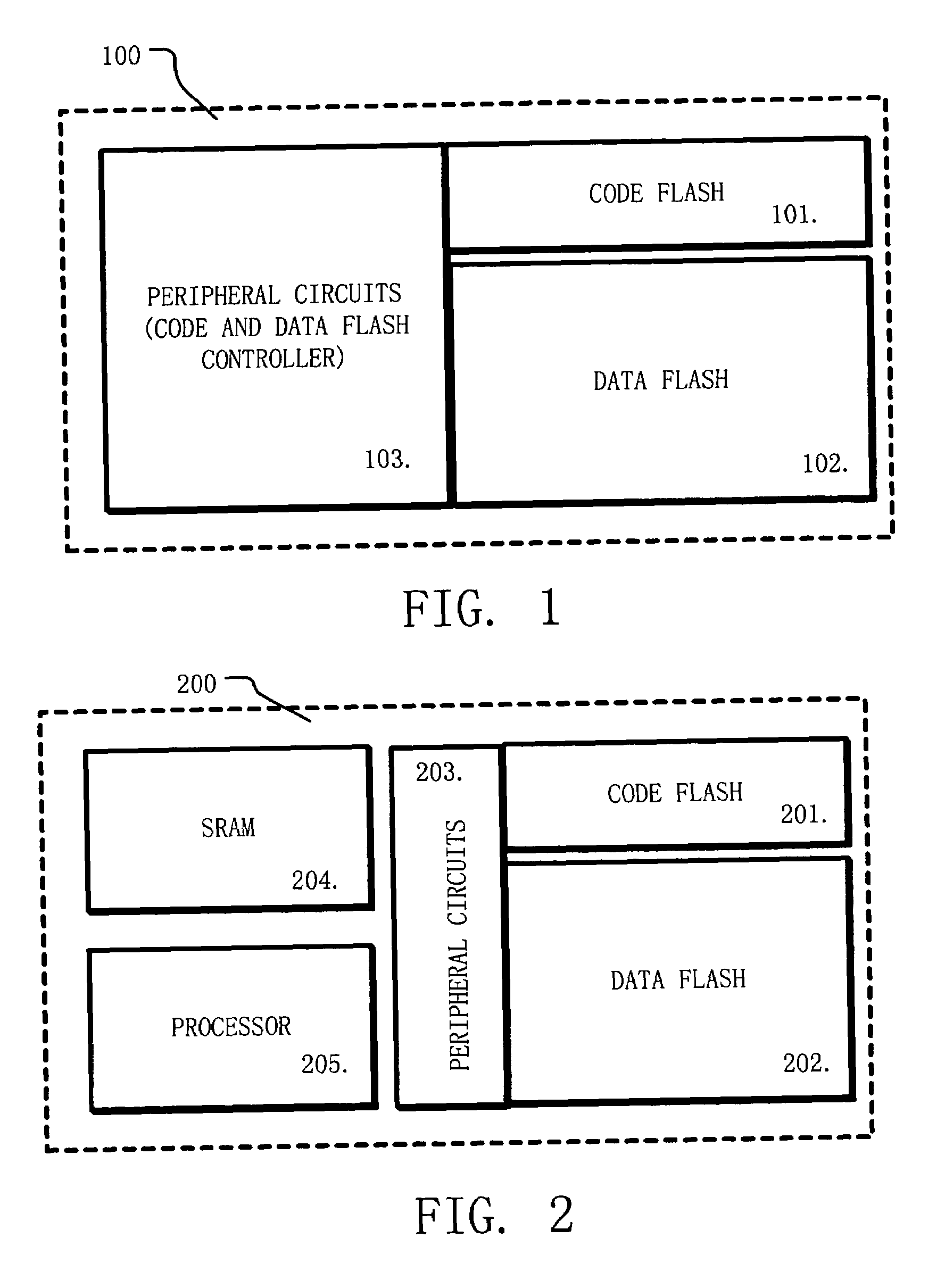
[0026]FIG. 1 illustrates the basic concept of the present invention. In particular, an integrated circuit 100 comprises a first memory array 101 adapted for code flash applications, and a second memory array 102 adapted for data flash applications. Peripheral circuits 103 on the integrated circuit include a code and data flash controller which execute first and second operation algorithms which are adapted for the patterns of data usage corresponding with code flash and data flash applications. In preferred embodiments, the memory cells in the first array 101 and the second array 102 have substantially the same structure, while the first and second operation algorithms differ to efficiently support different patterns of data usage within a single integrated circuit device.

[0027]The integrated circuit shown in FIG. 1 may include other components not shown in figure. For exampl...


PUM


Abstract

A memory architecture for an integrated circuit comprises a first memory array configured to store data for one pattern of data usage and a second memory array configured to store data for another pattern of data usage. The first and second memory arrays comprise charge storage based nonvolatile memory cells having substantially the same structure in both arrays. A first operation algorithm adapted for example for data flash applications is used for programming, erasing and reading data in the first memory array. A second operation algorithm adapted for example for code flash applications is used for programming, erasing and reading data in the second memory array, wherein the second operation algorithm is different than the first operation algorithm. Thus, one die with memory for both code flash and data flash applications can be easily manufactured using a simple process, at low cost and high yield.

Description

BACKGROUND OF THE INVENTION[0001]1. Field of the Invention[0002]The present invention relates to electrically programmable and erasable non-volatile memory and integrated circuits including such memory, and more particularly to architectures for such devices supporting both code and data flash.[0003]2. Description of Related Art[0004]Electrically programmable and erasable non-volatile memory technologies, including flash memory, are being adapted to many applications. Technologies based upon floating gates like standard EEPROM, or localized charge trapping structures like oxide-nitride-oxide memory cells known in various architectures as SONOS cells and NROM, are typically programmable and erasable many times. Flash memory technologies can be differentiated according to their use for storing data or code. Thus, market segments for so-called data flash and so-called code flash have developed.[0005]Data flash has several characteristics: (1) high density storage; (2) fast page program...

Claims


Application Information

Patent Timeline
Patent Type & Authority Patents(United States)
IPC IPC(8): G11C16/04H01L27/10G11C11/56G11C16/10G11C16/16H01L21/8247H01L27/115H01L29/788H01L29/792
CPCG11C16/0475G11C16/16G11C16/10
Inventor YEH, CHIH CHIEHTSAI, WEN JERLU, TAO CHENGLU, CHIH YUAN
Owner MACRONIX INT CO LTD
Why Eureka
Try Eureka