Memory and driving method of the same

a driving method and memory technology, applied in the field of memory and a driving method thereof, can solve the problems of imposing more burden on peripheral circuitry, and achieve the effects of reducing mounting area, improving yield, and dramatically increasing the reading speed of a memory

Active Publication Date: 2007-01-02
SEMICON ENERGY LAB CO LTD
View PDF6 Cites 61 Cited by
  • Summary
  • Abstract
  • Description
  • Claims
  • Application Information

AI Technical Summary

Benefits of technology

[0010]In Patent Document 2, a clocked inverter used as a sense amplifier is controlled by an input select signal which is supplied from outside. Thus, more burden is imposed upon peripheral circuitry.
[0011]According to the invention, mounting area is decreased and the yield is improved by decreasing the number of elements, and further a memory with less burden on peripheral circuitry and a driving method thereof are provided.
[0030]According to the invention in which the selection of the bit line and the amplification of a signal supplied from the memory cell are carried out simultaneously, reading speed of a memory is drastically increased. Compared to a sense amplifier which is used as an amplifier circuit of a memory in many cases, the invention using a clocked inverter having a small number of elements can contribute to improve the yield. Also, mounting area can be reduced due to the reduced number of elements, which allows further downsizing and weight saving. Furthermore, when compared to the case of using a sense amplifier which requires two inputs, the invention using a clocked inverter with one input can reduce the burden imposed upon peripheral circuitry because of the reduced signals to be controlled, which allows to reduce the number of lead wirings, for example.

Problems solved by technology

Thus, more burden is imposed upon peripheral circuitry.

Method used


Image

  • Memory and driving method of the same
  • Memory and driving method of the same
  • Memory and driving method of the same

Examples


embodiment mode 1

[Embodiment Mode 1]

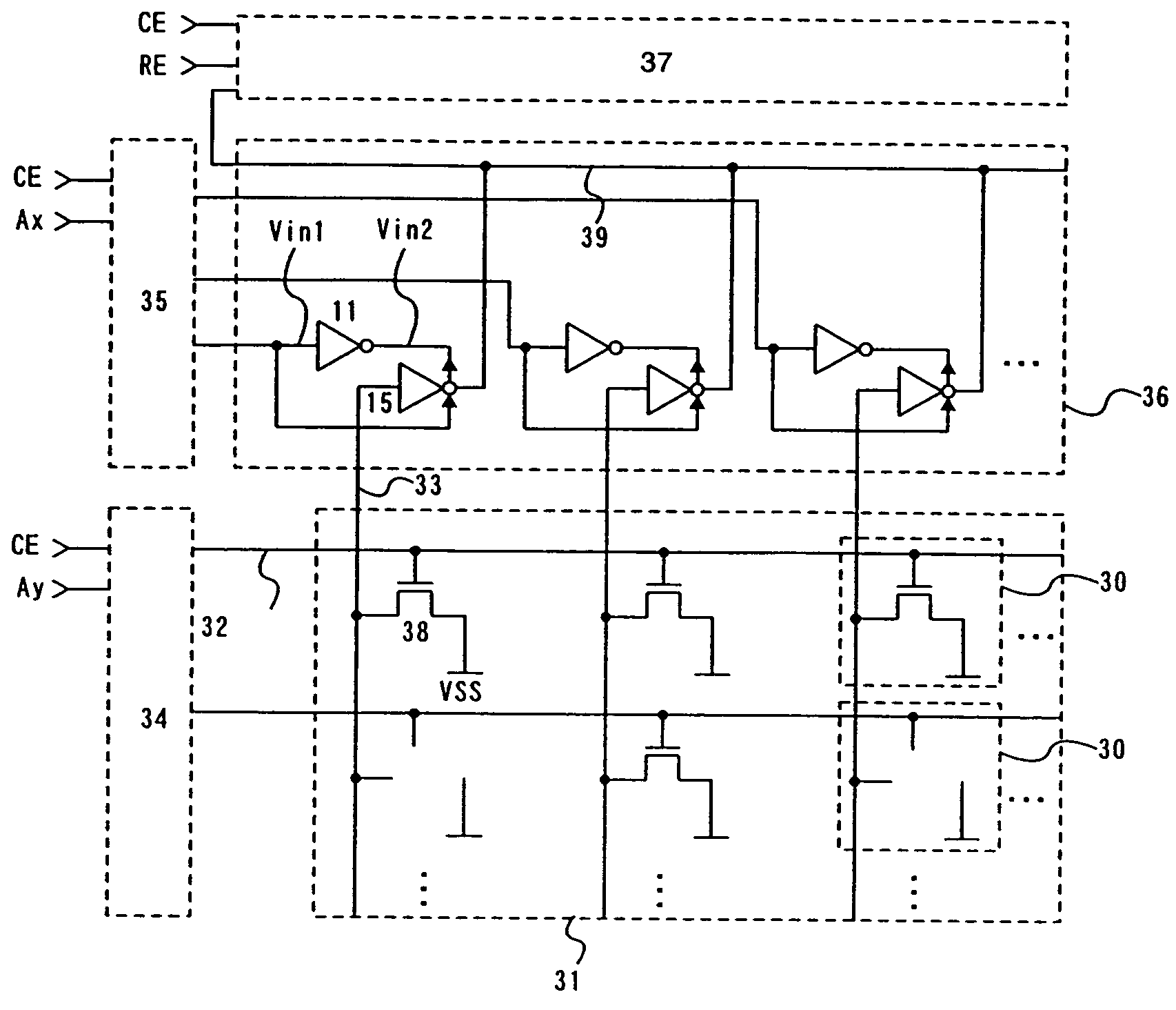
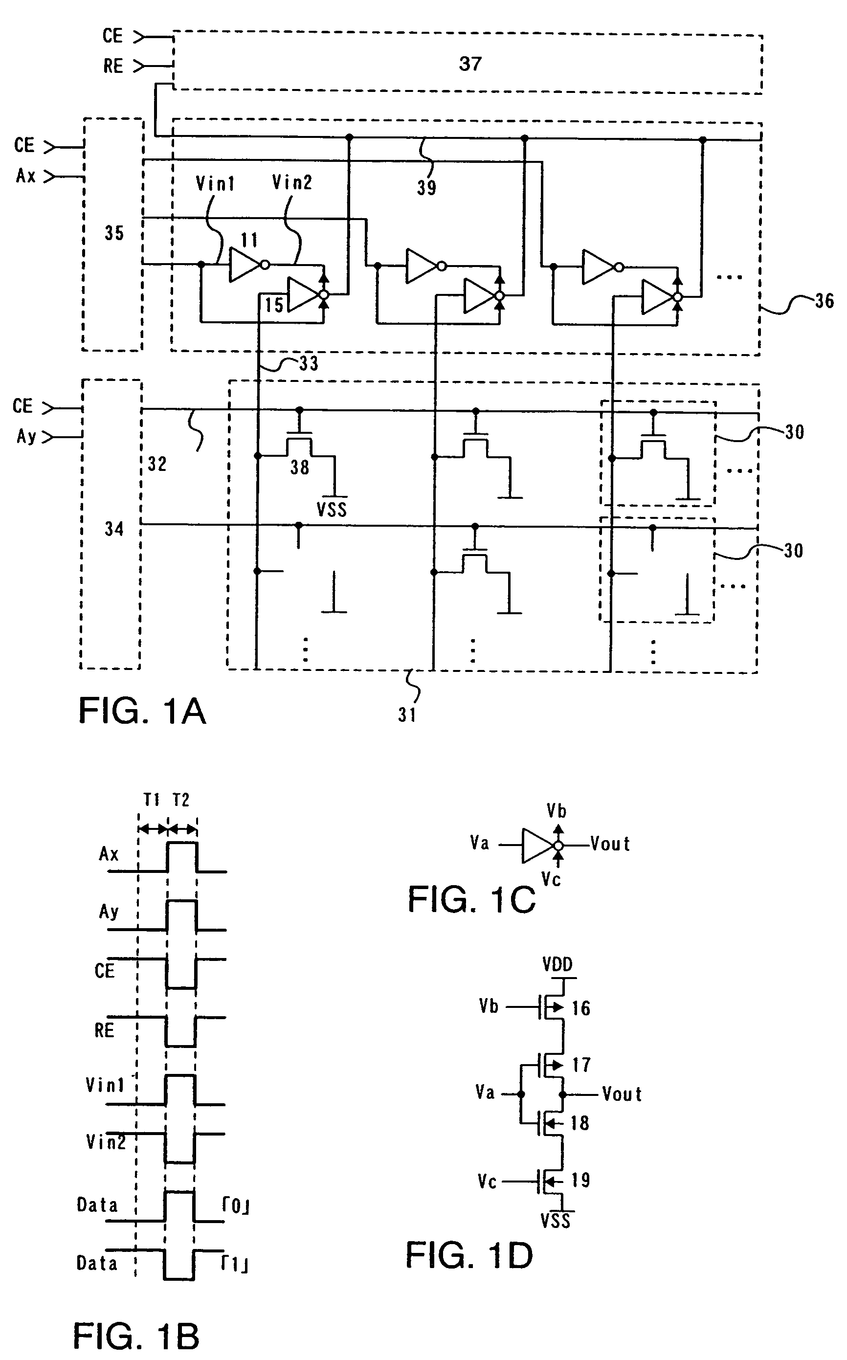
[0036]A configuration of a read only memory (typically a ROM) is described with reference to FIG. 1A as the memory of the invention.

[0037]The memory of the invention is provided with a memory cell array 31 in which memory cells 30 are arranged in matrix (in rows and columns). Further, a row decoder 34, a column decoder 35, a selector 36 and an output circuit 37 are provided, which control the operations of the memory cells 30.

[0038]The row decoder 34 is inputted with a Chip Enable signal (hereinafter referred to as a CE signal or CE) and an Ay signal. The column decoder 35 is inputted with a CE signal and an Ax signal. Note that a Read Enable signal (hereinafter referred to as an RE signal or RE) may be inputted to the both decoders although it is not shown.

[0039]The selector 36 is provided with an inverter 11 and a clocked inverter 15. The inverter 11 and the clocked inverter 15 are provided in each column corresponding to each bit line 33.

[0040]The clocked inver...

embodiment mode 2

[Embodiment Mode 2]

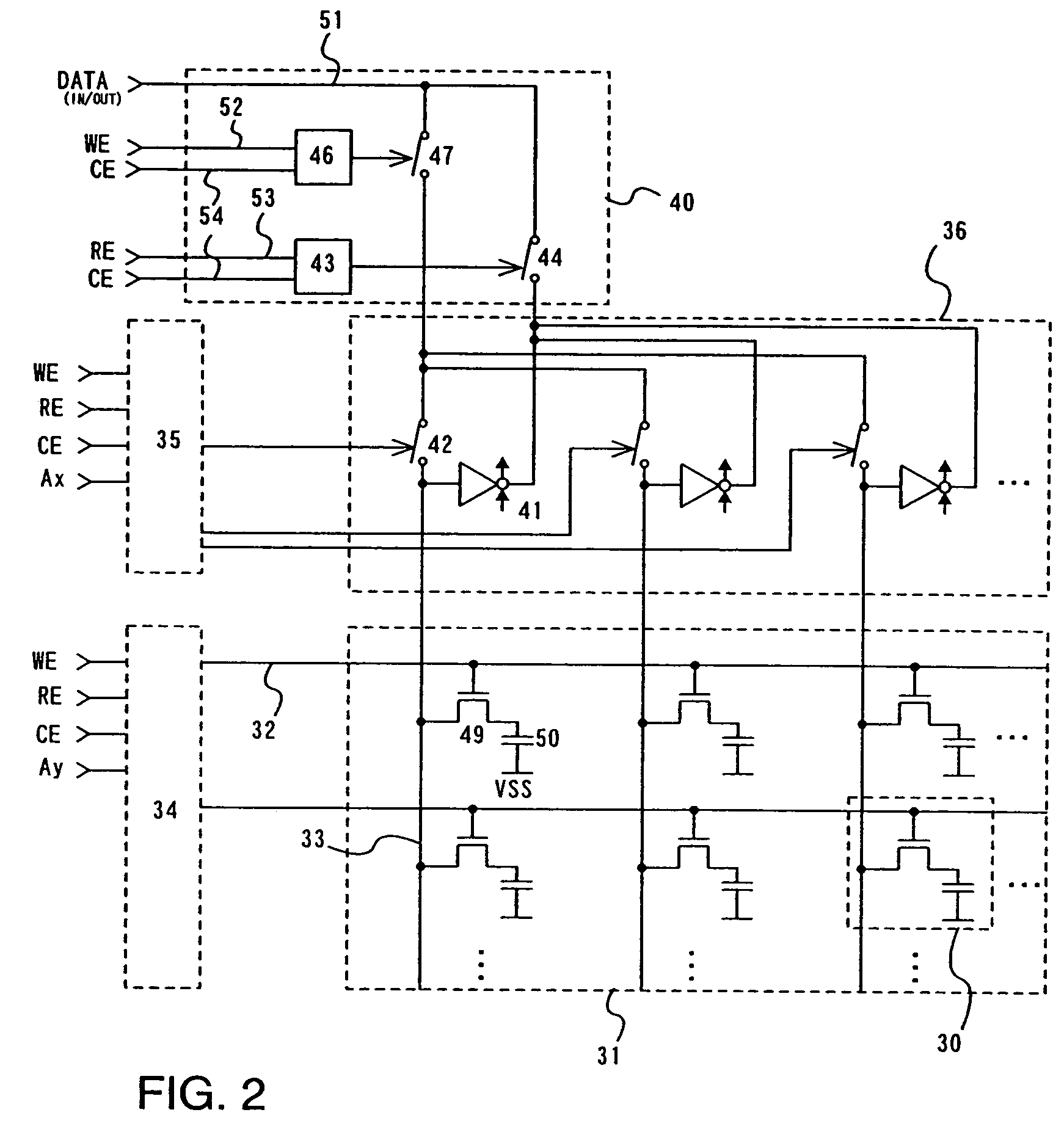
[0062]A configuration of a memory which is capable of reading and writing (typically a RAM) is described briefly with reference to FIG. 2 as the memory of the invention.

[0063]The memory of the invention comprises a memory cell array 31 in which memory cells 30 are arranged in matrix, a row decoder 34, a column decoder 35, a selector 36 and a Read / Write circuit (hereinafter referred to as a R / W circuit) 40. The selector 36 is provided with a clocked inverter 41 and a switch 42. The clocked inverter 41 and the switch 42 are provided in each column corresponding to each bit line 33. That is, assuming that the clocked inverter 41 and the switch 42 are one unit circuit, one unit circuit is provided corresponding to each bit line. Therefore, two unit circuits are provided in each column in the case where two bit lines (one is a bit line and the other is a bit bar line) are provided in each column.

[0064]The row decoder 34 is inputted with a Write Enable signal (hereinaft...

embodiment 1

[0085]A configuration example of a microprocessor (MPU) to which the invention is applied is described with reference to FIG. 4A. An MPU shown in FIG. 4A comprises a CPU 301, a main memory 303, a clock controller 304, a cache controller 305, a serial interface 306, an I / O port 307, a terminal 308, an interface 309, a cache memory 310 and the like on a substrate 300. The invention is applied to configurations of the main memory 303 and the cache memory 310, and driving methods thereof.

[0086]According to the aforementioned configuration, the substrate 300 may be formed of a silicon wafer, a quartz substrate, a glass substrate, a metal substrate, a stainless substrate, a plastic substrate and the like. When using a substrate formed of quartz, glass, metal, stainless material and the like, it is preferable to form each circuit by using an element comprising a polycrystalline semiconductor formed by a predetermined crystallization process after forming an amorphous semiconductor (a-Si) o...


PUM


Abstract

A memory having a bit line, a word line crossing the bit line, a memory cell electrically connected to the bit line and to the word line, a column decoder and a selector including a clocked inverter having a plurality of transistors electrically connected in series between a first power source and a second power source is provided. An input node of the clocked inverter is connected to the bit line, an output node of the clocked inverter is electrically connected to a data line, the plurality of transistors comprise a P-type transistor and a N-type transistor, a gate electrode of the P-type transistor and a gate electrode of the N-type transistor are electrically connected to the column decoder, and a sense amplifier is not interposed between the bit line and the input node of the clocked inverter.

Description

BACKGROUND OF THE INVENTION[0001]1. Field of the Invention[0002]The present invention relates to a memory and a driving method thereof. More particularly, the invention relates to a memory provided with a selector including a clocked inverter and a driving method thereof.[0003]2. Description of the Related Art[0004]In recent years, a memory is applied to a variety of fields such as a computer, a portable terminal, an IC card and further development is actively carried out. A memory comprises a plurality of memory cells arranged in matrix and peripheral circuitry including an output circuit.[0005]Some memories comprise a clocked inverter and a transistor which balances the potentials of an input node and an output node of the clocked inverter at an intermediate potential by short-circuiting both nodes and releases the short-circuit at the start of data transmission (For example, refer to Patent Document 1.). Further, the other circuits comprise a clocked inverter as a circuit for amp...

Claims


Application Information

Patent Timeline
Patent Type & Authority Patents(United States)
IPC IPC(8): G11C8/00G11C17/18G11C7/10G11C7/12G11C11/4094G11C11/418G11C11/419G11C17/08G11C17/12H03K17/00H03K17/687H03K17/693
CPCG11C7/1078G11C7/1096G11C17/12G11C11/4094G11C7/12
Inventor SHIONOIRI, YUTAKAATSUMI, TOMOAKIKATO, KIYOSHI
Owner SEMICON ENERGY LAB CO LTD
Why Eureka
Try Eureka