Magneto-resistive element

a magneto-resistive element and element technology, applied in the field of magneto-resistive elements, can solve the problems of increasing the reversal magnetic field, reducing the reproduction sensitivity brought about by an increase in coercivity, and affecting the reproduction sensitivity, so as to achieve the effect of suppressing the demagnetizing field

Inactive Publication Date: 2007-01-16
PANASONIC CORP
View PDF40 Cites 31 Cited by
  • Summary
  • Abstract
  • Description
  • Claims
  • Application Information

AI Technical Summary

Benefits of technology

[0011]According to a first aspect of the present invention, a vertical current-type magneto-resistive element includes an intermediate layer and a pair of magnetic layers sandwiching the intermediate layer, wherein one of the magnetic layers is a free magnetic layer in which magnetization rotation with respect to an external magnetic field is easier than in the other magnetic layer, wherein the free magnetic layer is a multilayer film including at least one non-magnetic layer and magnetic layers sandwiching the non-magnetic layer, and wherein an element area through which current flows is not larger than 1000 μm2, preferably not larger than 10 μm2, more preferably not larger than 1 μm2, most preferably not larger than 0.1 μm2. The element area is defined by the area of the intermediate layer through which the current flows perpendicular to the film plane. Providing the free magnetic layer as a multilayer structure of magnetic and non-magnetic layers suppresses the demagnetizing field, which increases as the element area becomes smaller. Here, the magnetic and non-magnetic layers can be single layers or multilayers. It is preferable that the free magnetic layer performs magnetization rotation at an external magnetic field causing magnetization rotation that is at least 50 Oe (ca. 4 kA / m) smaller than that required for magnetization rotation of the other magnetic layers (usually, the pinned magnetic layer). Especially when the element is used for a memory, it is preferable that magnetization rotation at a value of 10 to 500 Oe is possible.

Problems solved by technology

Therefore, there are the problems of Barkhausen noise due to magnetic wall transitions when used as a reproduction element, and instabilities of the switching magnetization when used for the memory operation of MRAMs.
On the other hand, in a region, in which the film thickness of the free magnetic layer with respect to the element area cannot be ignored, the demagnetizing field due to shape anisotropies becomes large, so that especially when used as a reproduction head, the decrease of the reproduction sensitivity brought about by an increase of the coercivity becomes a problem.
When used as an MRAM, the increase of the reversal magnetic field becomes a problem.
In previously proposed methods for reading non-volatile MRAM elements, the read-out is difficult when there are large variations in element resistance or in the resistance of switching element and electrode, because what is read out is the change of magnetic resistance of the magneto-resistive element with respect to the total resistance of magneto-resistive elements connected in series to a switching element and an electrode.
In order to improve the S / N, a method of reading an element with the voltage between that element and a reference element has been proposed, but in that case, the higher integration of the elements becomes a problem, because the reference element is necessary (see p.

Method used


Image

  • Magneto-resistive element
  • Magneto-resistive element
  • Magneto-resistive element

Examples


working example 1

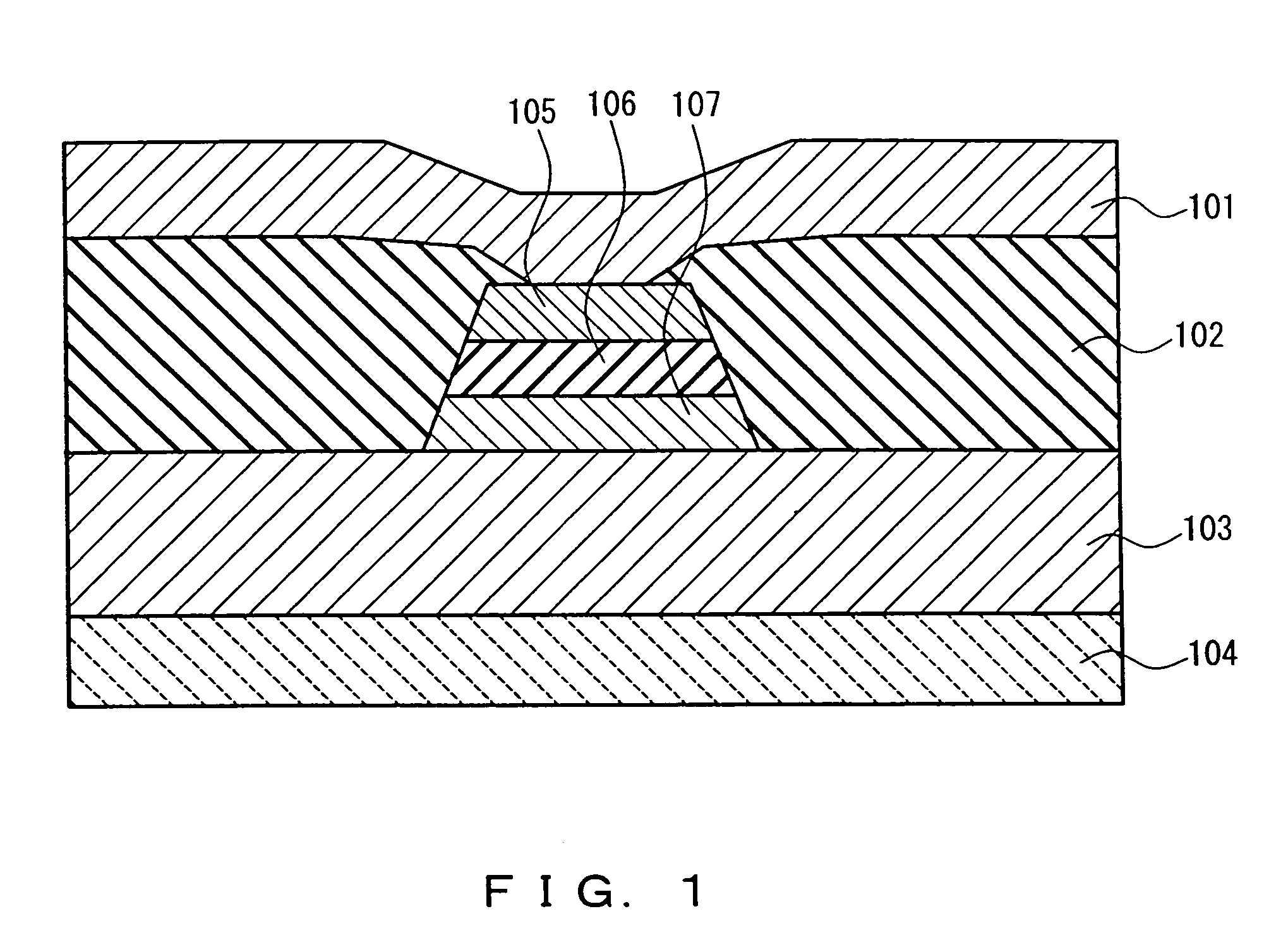
[0122]The following MR elements were produced by magnetron sputtering on a thermally oxidized Si substrate. The general configuration of these elements is shown in FIG. 1.

Sample 1

[0123]Ta(3) / Cu(500) / Ta(3) / PtMn(30) / CoFe(3) / Ru(0.7) / CoFe(3) / Al2O3(1) / NiFe(8) / Ta(3)

Sample 2

[0124]Ta(3) / Cu(500) / Ta(3) / PtMn(30) / CoFe(3) / Ru(0.7) / CoFe(3) / Al2O3(1) / NiFe(4) / Ta(3) / NiFe(4) / Ta(3)

Sample 3

[0125]Ta(3) / Cu(500) / Ta(3) / PtMn(30) / CoFe(3) / Ru(0.7) / CoFe(3) / Al2O3(1) / NiFe(5) / Ru(0.7) / NiFe(3) / Ta(3)

[0126](The numbers in parentheses indicate the film thicknesses in nm. The film configuration is noted starting at the substrate side. This is also true in the following.)

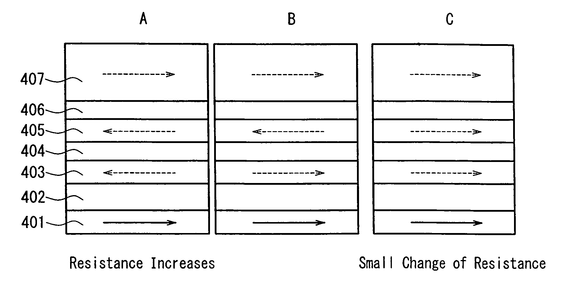
[0127]Here, Ta(3) / Cu(500) / Ta(3) serves as a lower electrode and primer layer 103 on a substrate 104, PtMn is an antiferromagnetic layer (not shown), CoFe(3) / Ru(0.7) / CoFe(3) is a pinned magnetic layer 107, Al2O3 is the intermediate layer 106, and the rest serves as the free magnetic layer 105 (and the last layer Ta(3) as the protective layer).

[0128]The para...

working example 2

[0151]The following elements were produced by magnetron sputtering on a thermally oxidized Si substrate.

Sample 1

[0152]Ta(3) / Cu(500) / Ta(3) / CoFe(32) / Al2O3(X) / CoFe(3) / Ru(0.7) / CoFe(3) / PtMn(20) / Ta(3)

Sample 2

[0153]Ta(3) / Cu(500) / Ta(3) / (CoFe(4) / Ta(3) / CoFe(4))*4 / Al2O3(X) / Fe(3) / Ru(0.7) / CoFe(3) / PtMn(20) / Ta(3)

Sample 3

[0154]Ta(3) / Cu(500) / Ta(3) / (CoFe(3) / Ru(0.7) / CoFe(5))*4 / Al2O3(X) / CoFe(3) / Ru(0.7) / CoFe(3) / PtMn(20) / Ta(3)

[0155]Here, (CoFe(4) / Ta(3) / CoFe(4))*4 means that the layers (CoFe(4) / Ta(3) / CoFe(4)) are produced four times in repetition.

[0156]The multilayer films were microprocessed using photolithography into mesa shapes with an element area of 2×5, 10×25, 20×50, and 40×100 μm2, and after forming an inter-layer insulator film, an upper electrode was formed, yielding vertical current-type magneto-resistive elements with the cross section shown in FIG. 7 and FIG. 8. In these elements, the free magnetic layer 105 is arranged on the substrate side, different from FIG. 1. The film thickness X of the...

working example 3

[0160]The following sample was produced by magnetron sputtering on a thermally oxidized Si substrate.

[0161]Ta(3) / Cu(500) / Ta(3) / PtMn(30) / CoFe(3) / Ru(0.7) / CoFe(3) / Al2O3(1.5) / CoFe(d1) / Ru(0.7) / NiFe(d2) / Ta(3)

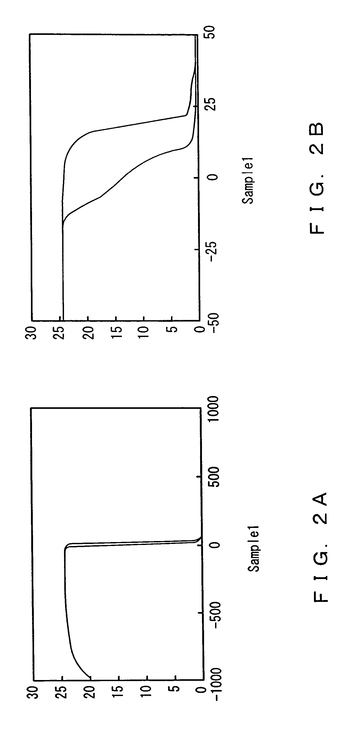
[0162]Multilayer films with this configuration were microprocessed using photolithography into mesa shapes with an element area of 2×2 μm, and after forming an inter-layer insulator film, an upper electrode was formed, yielding a vertical current-type magneto-resistive element with the cross section shown in FIG. 1. The parameters for the thermal processing were a temperature of 260° C., a magnetic field of 5 kOe, and a time of 1.5 h. Then, the MR when applying magnetic fields of ±200 Oe to the resulting element was measured, and the change of the MR in a relatively small external magnetic field was examined. The results are shown in Table 2. With the saturation magnetization M1 of CoFe being 2.15 T and the saturation magnetization M2 of NiFe being 1 T, CoFe has the higher spin polari...


PUM

PropertyMeasurementUnit
areaaaaaaaaaaa
thicknessaaaaaaaaaa
thicknessaaaaaaaaaa

Abstract

The present invention provides a vertical current-type magneto-resistive element. The element includes an intermediate layer and a pair of magnetic layers sandwiching the intermediate layer, and at least one of a free magnetic layer and a pinned magnetic layer is a multilayer film including at least one non-magnetic layer and magnetic layers sandwiching the non-magnetic layer. The element area defined by the area of the intermediate layer through which current flows perpendicular to the film is not larger than 1000 μm2.

Description

[0001]This application is a divisional of application Ser. No. 09 / 931,113, filed Aug. 16, 2001 now U.S. Pat. No. 6,767,655, which application is incorporated herein by reference.BACKGROUND OF THE INVENTION[0002]1. Field of the Invention[0003]The present invention relates to magneto-resistive elements that are widely used, for example, in magnetic random access memory (MRAM) used in data communication terminals, for example, and to manufacturing methods for the same.[0004]2. Description of the Related Art[0005]It is known that when a current flows through a multilayer film including ferromagnetic material / intermediate layer / ferromagnetic material in a direction traverse to the intermediate layer, a magneto-resistive effect occurs due to the spin tunneling effect if the intermediate layer is a tunneling insulating layer, and a magneto-resistive effect occurs due to the CPP (current perpendicular to the plane)-GMR effect if the intermediate layer is a conductive metal, such as Cu. Both...

Claims


Application Information

Patent Timeline
Patent Type & Authority Patents(United States)
IPC IPC(8): G11B5/39G01R33/09G11C8/02H01F10/14H01F10/16H01F10/32H01F41/18H01F41/30H01L21/8246H01L27/105H01L27/22H01L43/08H01L43/12
CPCB82Y10/00B82Y25/00B82Y40/00H01F10/3268H01F10/3272H01F41/302H01L43/08H01L43/12Y10T428/1129Y10T428/1193Y10T428/1121Y10T428/1143Y10T428/1107H01L27/228H10B61/22H10N50/01H10N50/10H01F10/14
Inventor HIRAMOTO, MASAYOSHIMATUKAWA, NOZOMUODAGAWA, AKIHIROIIJIMA, KENJISAKAKIMA, HIROSHI
Owner PANASONIC CORP
Why Eureka
Try Eureka